Academic year 2019-2020
European Master of Science in Photonics
Master's dissertation submitted in order to obtain the academic degree of Counsellors: Sheng Yang, Prof. dr. Johan Lauwaert
Supervisors: Prof. dr. Johan Lauwaert, Prof. Stefaan De Wolf (KAUST) Student number: 01800687
Suraj Manikandan
Suraj.manikandan@ugent.be
Faculty of Engineering and Architecture
Department of Electronics and information systems Ghent University
Place for Project
Technologiepark Zwijnaarde 126 9052 Zwijnaarde
Examiner
Prof. dr. ir. Filip Strubbe Prof. dr. ir. Peter Bienstman
Prof. dr. ir. Benoit Bakeroot(External) Ghent University
Supervisor
Prof. Johan Lauwaert
Prof. Stefaan De Wolf[KAUST] Place
The rapid development of the economy ultimately increases energy demand. An investigation from the World energy forum indicated that everyday human species consume its way through more than a million terajoules of energy. So this shows the importance of renewable energy since energy from sum is unlimited and we need a device to convert sun energy to a much usable form. Since the first perovskite solar cell was introduced in the year 2009 with an efficiency of less than 4% since the research was Began in the year of 2006. The reason for the less stable solar cell was due to the corrosive liquid phase that slowly disrupted other layers within the device. By 2012 the liquid phase component was replaced with the solid-state contacts and the new efficiency was improved to 10%. Continuous improvement in device physics and the investigation of new materials fabrication methods lead to an efficiency of 25% in the year 2019. The power converts ion efficiency of perovskite solar cells already exceeds the traditional thin-film photovoltaics such as CIGS, CdTe.
The main theme of this thesis is to perform detailed interface-defect studies on a series of relevant perovskite solar cells. Specific emphasis will be laid on the characterization of sub-bandgap states, characterized by methods such as deep-level transient spectroscopy. In chapter 1 we presented an overview of the perovskite solar cell since it is a new technology, we discussed the bandgap tuning, passivation of devices for better efficiency. In chapter 2 we introduce the characterization method like IV, CV, EQE measurement, with the detailed working principle. Found the SRH recombination energy which degraded the performance of solar cells under low temperature. In chapter 3 Studied the defect in the solar cell by admittance spectroscopy, Capacitance spectroscopy, or more generally also know as admittance spectroscopy provide a deep insight into the carrier dynamics in the diode like a device like a solar cell. In this spectroscopy differential capacitance is measured, differential capacitance is the charge response δQ, to a very small change in voltage
capacitance under varying temperatures. Since from the semiconductor principle, defect states in the band-gap will respond to the given signal. Trap levels present in perovskite with activation energies varied in the range of 0.13 - 0.23 eV above the valence band was found and it’s been identified as perovskite defect. The capacitance behavior gives significant information about the defect density, capture cross-section of the holes, lifetime of holes. In Chapter 4, we did two spectroscopy techniques in this chapter, Thermally stimulated current spectroscopy is used to reveal a broad trap distribution, instead of the discrete trap level. TCS behavior can only be seen at a specific temperature. In contrast, DLTS analysis is based on the sampling of the diode capacitance, since capacitance transient is obtained by changing the applied voltage from a reverse value to approximately zero. The second one is Temperature-dependent space charge limited current spectroscopy (TDSCLC) which is quite famous with an organic solar cell, but we tried this method the found the defect density energy at 130 meV. In Chapter 5, Steady-State Photocarrier Grating Method(SSPG) principle is The SSPG method is based on the carrier diffusion under the presence of spatial sinusoidal modulation in the photogeneration rate (G), which induces a photocarrier grating. From photocurrent measurements at different grating periods (λ), the ambipolar diffusion length Ldcan be determined by an analysis that assumes ambipolar transport and charges neutrality. we found the diffusion length as 180 nm. In Chapter 6, we conclude with a numerical model, for which in the earlier chapter we did the experiments. The SCAPS model we made can simulate the I-V, C-V, C-F curves from a temperature range of 300-260k. Also presented an advance concept of perovskite solar cell using the microlens.
I started my thesis very late as compared to my fellow mates. Despite this hard year of COVID 19, I liked to work on this master thesis and consider as one of the best decisions i made so far in my life. This was an experience that allowed me to grow as a researcher and more as a person. All of this is would be impossible without a nice and large number of people who supported me over my master thesis.
Firstly I want to thank Prof. Johan Lauwaert, my promoter. He is very professional and he has given me a considerable amount of help during my thesis in Ghent. I appreciate the knowledge he shared with me for the modeling of perovskite solar cells and he always cleared all my doubts even the silliest. Your Socratic method made me a more critical master research student and made sure I was an incorrect path where I can find the right answer. A special acknowledgment Prof. Stefaan De Wolf, without the solar cell this thesis is nothing. KAUST solar center made all the perovskite solar cells for the experiment which we did in Ghent. I am deeply in debt to Sheng Yang, she helped me the experiments. Even she clears all my doubts related to any apparatus in the ELIS solar lab. She helped me with the preparation of the master thesis manuscript.
My biggest thanks to Erkan Aydin from King Abdullah University of Science and Technology helping me with the perovskite material modeling. I have always found your door open whenever I needed help and guidance and discussion with you have always been enlightening. Your contagious enthusiasm helped me get past what seemed then like obstacles. Thanks for the good management, I also want to thank your research group for the one of the best perovskite solar cells.
1.1.1 Comparative primary energy consumption over the past 15 year[18] . . 3
1.1.2 90% of the city of Rotterdam lies below sea level, leaving many residential areas vulnerable to a rising ocean.[49] . . . 5
1.1.3 The 300 MW Sakaka PV project.[8] . . . 6
1.2.1 Renewable energy generation, Belgium, 1965 to 2018[82] . . . 8
1.3.1 Classification of Photovoltaic technologies . . . 9
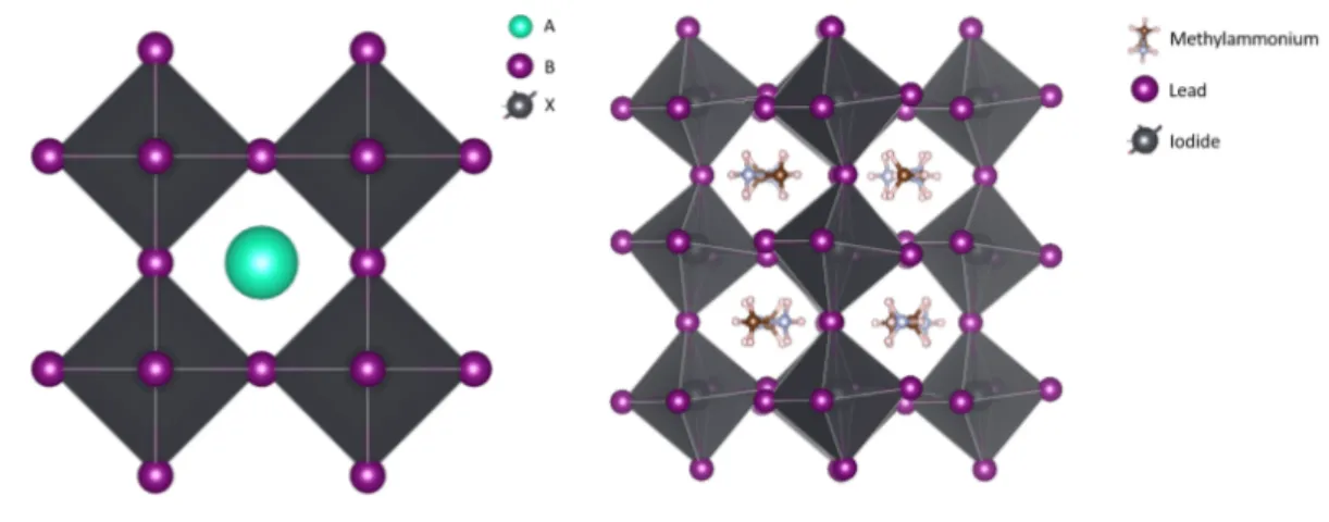
1.4.1 A generic perovskite crystal structure of the form ABX3and F AP bI3. . 11
1.5.1 Classification of perovskite. . . 13
1.5.2 Example perovskite structures for Inorganic Perovskite . . . 14
1.5.3 Halide based perovskites structure . . . 14
1.6.1 Perovskite solar cells have increased in power conversion efficiency at a phenomenal rate compared to other types of photovoltaics. Although this figure only represents lab-based ”hero cells”, it heralds great promise.[55] . . . 15
1.6.2 The maximum photon energy utilisation (defined as the open circuit voltage Voc divided by the optical bandgap Eg) for common single junction solar cells material systems.[3] . . . 16
1.6.3 UV–vis absorbance and band-gap values CH3N H3P bX3, X=I,Cl,Br. . . 18
1.6.4 Comparative study of absorption peak of different perovskite with different metal anion. . . 19
1.7.1 Classification of fabrication method for perovskite solar cell . . . 20
1.7.2 Spin coating technique followed by baking process. . . 21
1.7.3 Approximation of thin-film deposition via spray coating[90] . . . 22
1.7.4 Vapor deposition of perovskite layers . . . 23
1.8.1 The three pillars of successful commercial solar cells . . . 24 1.8.2 Ball and stick models showing A-cation candidates used in perovskites. 26
1.8.3 UV-curable epoxy applied to a perovskite solar cell and then sealed with a glass cover slip[78]. . . 27 2.1.1 (a)Band profile of p,i,n-type semiconductor in isolation.(b) Band profile
of p-i-n junction in equilibrium . . . 29 2.1.2 Electric field dropping across i layer with background impurities. The
dashed line shows the electric field distribution at the point where the i region is just depleted as this line doesn’t end near n-type due to asymmetrical thickness of P and n layer. . . 30 2.2.1 Layer width of p-i-n junction structure. . . 30 2.3.1 Current-voltage characteristic of perovskite solar cell in dark . . . 34 2.3.2Current-voltage characteristic of perovskite solar cell in dark with
temperature sweep . . . 34 2.3.3 Current-voltage characteristic of perovskite solar cell in dark and light 35 2.3.4Maximum efficiency limit of solar cell . . . 36 2.3.5 Maximum power point calculation in solar cell. . . 37 2.3.6Equivalent circuit of solar cell with series and shunt resistance . . . 38 2.3.7 Effect of (a) decreasing series resistance and (b) increase in shunt
resistance. . . 38 2.3.8SRH recombination through the acceptor defect (a . . . 40 2.4.1 Representation of the different stages of the generation of the
photo-current in Pervoskite n-i-p device. (a) photons entering the device; (b) formation of electron hole pair(exciton);(c) Separation and travelling of charge to the contact; (d) Collection of charge at the contacts. . . 41 2.4.2Generic structures of (a)conventional (b) inverted planar . . . 42 2.5.1 Getting to the working point and first calculation point . . . 45 2.6.1 Schematic of a solar simulator for J-V measurements under illumination
with a spectrum resembling the standard AM1.5G. . . 47 2.6.2Perovskite solar cell measured using a four probe setup. . . 47 2.6.3(a)Dark I–V plots displayed in log-linear scale for deep analysis of the
rectifying perovskite device structures (b) Current-voltage curves of perovskite with varying lifetime . . . 48 2.6.4Temperature dependence of the open-circuit voltage Voc FAMA
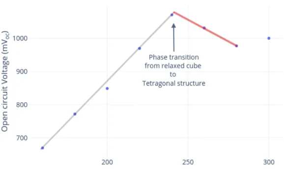
perovskite with a bandgap of 1.48 eV . . . 50 2.6.5 Absorption losses in glass for solar cell application . . . 52
2.6.6A schematic diagram of the spectral response measurement setup used in ELIS . . . 53 2.6.7 EQE measurement of FAMA perovskite solar cell . . . 53 3.0.1 Temperature-Sweeping Capacitive Techniques to Evaluate Band-Gap
Defect Densities in Perovskites . . . 56 3.2.1 (a) Energy-band diagram of the perovskite material representing the
carrier recombination and trapping processes. (b) AC electrical equivalent circuit of the perovskite solar cell[56] . . . 58 3.3.1 Capacitance spectra measured in open-circuit conditions for different
illumination intensities between 100 Hz and 10 MHz . . . 60 3.3.2 (a) Accumulation capacitance vs varying intensity of illumination,
proportionality between capacitance with illumination; (b) Open circuit voltage with the accumulation capacitance, with the slope equal to thermal voltage. . . 61 3.3.3 (a) Depletion layer at equilibrium; (b) Generation of minority carriers
produces flat band condition and further accumulation (c) The total open-circuit voltage is the increase in minority carrier Fermi level. . . . 61 3.4.1 capacitance-voltage profile . . . 63 3.4.2(a) Temperature dependant capacitance-voltage profile (b) Doping
profile of PSC’s for different temprature . . . 64 3.5.1 Admittance spectroscopy: capacitance and conductance for device
architecture . . . 65 3.5.2 (a) Temperature dependence of capacitance-frequency, (b) DOS spectra
which shows the characteristic frequency at each temperature, . . . 66 3.5.3 Arrhenius plot of the characteristic frequencies to extract the defect
activation energy and the defect energy distribution of formaldehyde perovskite. . . 67 3.6.1 Compression between the DLCP measurement with the CV profiling at
low and high frequency. . . 69 4.3.1 Flow diagram representing the experiment procedure . . . 72 4.4.1 Heating rate dependence of TSC spectra in the temperature range of
120–300 K measured from 0.10 to 0.40 K/s for perovskite solar cell with illumination it shows the Two TSC peak . . . 73
4.5.1 Bias-dependent TSC spectra measured from 0.5 to 2 V for FAMA perovskite sample. . . 74 4.5.2 Density of states(DOS) for the TSC peak at 170meV with the capture
cross section 40X10−16cm2 . . . 75 4.5.3 Density of states(DOS) for the TSC peak at 580meV the capture cross
section 40X10−16cm2 . . . . 76
4.8.1 (a) Space-charge-limited-current (SCLC) density vs applied voltage at different temperatures (b) J(U) at 300 K with straight line indicates the Ohmic behavior of thermally generated charge carriers. . . 78 4.8.2Current density for a fixed applied voltage U with the inverse
temperature, the straight line indicates the activation energyEA(U ) . . 79 4.8.3Density of states above the valence band for perovskite solar cell . . . . 80 5.2.1 Schematics of the interference experiment with two plane waves
L1andL2, In (a) there will be no interference can be seen (b) there will
be interference due the two plane wave. . . 83 5.3.1 Schematics of experimental setups with order to change the angle
between the two beams . . . 85 5.4.1 Two coherent laser beams form a laser grating, the period of which (Λ)
can be controlled by changing the angle between the two beams. . . 86 5.4.2 The conductivity ratio and grating period are plotted in a linear manner;
a steeper slope corresponds to a higher ambipolar diffusion length. The blue lines are linear fits of equation with the slope of 1.8. . . 87 5.5.1 The measured photoconductivity as a function of the photon flux,
plotted on a double logarithmic scale. The fitted dashed lines reveal a power law behavior from which the parameterγ is extracted. . . . 88 6.2.1 UV–vis absorbance and band-gap values CH3N H3P bX3, X=I,Cl,Br all
these calculation were performed using Quantum ATK. . . 93 6.2.2Variation of FF and PCE with thickness of perovskite . . . 94 6.3.1 Structural diagram of perovskite with there respective thickness of each
layer . . . 95 6.3.2(a) comparative result I-V measurement of the simulation with
experiment result at 300k (b) comparative result I-V measurement of the simulation with experiment result at 280k . . . 97
6.3.3Comparison between the simulated and experiment capacitance voltage profiling . . . 98 6.3.4Comparison between the simulated and experiment capacitance
frequency. . . 99 6.4.1 Processes of making lenses by melting photo-resist. ( a ) Simple melting;
( b ) pre-forming the resist.[21] . . . 100 6.4.2Profilometer measurement of a perfect lens through resist melt technique.102 6.4.3Profilometer measurement of a deformed lens through resist melt
technique, here lens got collapes due to the high surface tension and height . . . 102 6.4.4Compassion between the Current-voltage measurement with solar
1.2.1 Merits and demerits of solar cell . . . 8
1.3.1 Merits and demerits of different solar cell technologies . . . 10
1.4.1 The perovskite ’name-picking’ table . . . 11
1.6.1 The bandgap, energy loss, and open-circuit voltage of solar cells . . . . 17
1.6.2 Band gap of perovskites with variation based on A site cations. . . 17
2.6.1 Table shows the temperature with corresponding Vocand Isc . . . 49
2.7.1 Physical characteristics of perovskite solar cells as extracted under various condition . . . 54
3.7.1 Summary of trap parameters for the admittance spectroscopy of formamidinium N-i-P perovskite devices. . . 69
5.6.1 Derived parameters from the SSPG and photoconductivity measurements. 89 6.3.1 Photovoltaic characteristics of PSC used in the simulation. . . 96
6.3.2Defect characterization in perovskite solar cell . . . 96
6.3.3Comparison between simulated and experiment data . . . 98
I
Background
1
1 Introduction
2
1.1 Energy Issues . . . 2
1.1.1 Global warming and health problems . . . 3
1.1.2 Non-renewabality . . . 5
1.2 The huge potential of solar energy . . . 8
1.3 Photovoltaic Technology(PV) . . . 9
1.3.1 Mono-crystalline and Poly-crystalline Photovoltaic Technology . 9 1.3.2 Thin Film Photovoltaic Technology . . . 10
1.4 Perovskite . . . 11
1.5 Classification of perovskite system . . . 13
1.5.1 Inorganic Perovskite . . . 13
1.5.2 Halide perovskite . . . 14
1.6 Why are Perovskite Solar Cells So Significant? . . . 15
1.6.1 Band gap engineering . . . 17
1.6.2 Lead replacement in organometal halides . . . 18
1.7 Fabrication method for perovskite solar cell . . . 20
1.7.1 Solution Processing-Based Techniques . . . 20
1.7.2 Vapour based technique . . . 22
1.8 Challenges of Perovskite Solar Cell . . . 24
1.8.1 Instability and degradation . . . 24
1.8.2 Methods of Increasing Stability and degradation . . . 26
2 Thin-film perovskite photovoltaics and SCAPS 1D
28
2.1 P-i-N junction . . . 282.3 Characteristic of photovoltaics . . . 33
2.3.1 Quantum efficiency and photo-current . . . 33
2.3.2 Dark current and open-circuit voltage . . . 33
2.3.3 Efficiency . . . 35
2.3.4 Parasitic resistance . . . 37
2.3.5 Nonradiative Recombination . . . 39
2.4 Perovskite solar cell construction and working . . . 40
2.4.1 Working principle . . . 40
2.4.2 Device Structures of Perovskite Photovoltaics Devices . . . 41
2.5 SCAPS-1D Numerical simulation . . . 43
2.5.1 Grading Models in SCAPS-1D . . . 44
2.5.2 Working theory . . . 45
2.5.3 Merits and demerits . . . 45
2.6 Electrical characterization methods of perovskite solar cell . . . 46
2.6.1 Measurement of Current-Voltage Curves . . . 46
2.6.2 Current-Voltage curves . . . 46
2.6.3 Temperature dependent Current-Voltage Measurements . . . . 49
2.6.4 Quantum Efficiency Measurements . . . 50
2.6.5 Measurement Principle and Calibration . . . 52
2.7 Conclusion . . . 52
II
Electric Characterization
55
3 Capacitance Spectroscopy
56
3.1 Introduction . . . 563.2 Admittance origin. . . 57
3.3 Light induced space charge accumulation zone in perovskite solar cell 59 3.4 CV Profiling and the Depletion Approximation . . . 62
3.5 Admittance response of trap states . . . 63
3.6 Influence of deep level states on CV profiles . . . 67
3.7 conclusion . . . 69
4 Current spectroscopy techniques
70
4.1 Introduction . . . 704.3 Experiment procedure . . . 71
4.4 The effect of heating rate on TSC spectrum . . . 72
4.5 The effect of bias voltage on TSC spectrum . . . 74
4.6 Temperature dependent space charge limited current spectroscopy (TDSCLC) . . . 76
4.7 Methodology . . . 76
4.8 Results . . . 78
4.8.1 Density of states in perovskite thin film . . . 78
III
Optical Characterization
81
5 Laser induced Steady-State Photocarrier Grating Method
82
5.1 Introduction . . . 825.2 Basic principle . . . 83
5.3 Experimental Setup . . . 84
5.4 Diffusion length calculation . . . 84
5.5 Minority-majority carrier and mobility lifetime products . . . 87
5.6 conclusion . . . 89
IV
Numerical model
90
6 Solar Cell Capacitance Simulator model and future aspect of
perovskite solar cell
91
6.1 Introduction . . . 916.2 Perovskite . . . 91
6.2.1 Electronic Behavior . . . 92
6.2.2 Ambipolar conductivity . . . 92
6.2.3 Optical properties . . . 92
6.2.4 Defects in perovskites: intrinsic/point defect . . . 93
6.3 Device modelling using SCAPS 1D . . . 94
6.3.1 SCAPS parameters . . . 95
6.3.2 Current voltage characterization . . . 96
6.3.3 Capacitance voltage characterisation . . . 97
6.3.4 Capacitance frequency characterization . . . 99
6.4.1 Micro concentrator Perovskite solar cell . . . 99 6.4.2 Fabrication of micro lens . . . 100 6.4.3 Result . . . 101
Introduction
““We are like tenant farmers chopping down the fence around our house for fuel when we should be using Natures inexhaustible sources of energy – sun, wind and tide. … I’d put my money on the sun and solar energy. What a source of power! I hope we don’t have to wait until oil and coal run out before we tackle that.””
—Thomas Edison (1877–1930), Inventor and businessman
1.1
Energy Issues
The rapid development of the economy ultimately increases energy demand. An investigation from the World energy forum indicated that everyday human species consume its way through more than a million terajoules of energy. It is equivalent to if all of us boiled 70 kettles of water an hour around the clock. With the global population increasing and industrialization on the rise in developing nations, there is a hunger for energy has reached unprecedented levels[34]. More than half of our energy comes from fossil fuel such as natural gas and crude oil.
It is estimated that since commercial oil drilling began in the 1850s, we have sucked up more than 135 billion tonnes of crude oil to drive our cars, fuel our power stations and heat our homes[35]. That figure increases every day. Due to this increase in consumption in fossil fuel, cause an issue of depletion of fossil fuels with environmental pollution and global warming have raised significant concerns as well. Due to dramatic expansion in energy use which entails severe consequences. The drawbacks and problems are listed underneath.
Figure 1.1.1: Comparative primary energy consumption over the past 15 year[18]
1.1.1
Global warming and health problems
The burning of fossil fuels has increased the amount of CO2and greenhouse gas in the
atmosphere. This results in serious alterations to the environment, eventually cause problems for human health. This will also cause a change in precipitation patterns in many areas to cause, risk of droughts and floods, and rise in sea level, leading to the loss of coastal land. The World Health Organization (WHO) reports that climate change is responsible for at least 150,000 deaths per year, a number that is expected to double by 2030[75].
Heatwaves
The high expose of abnormally high temperatures can have serious health effects on the human population, such as the elderly and the sick. This was already seen during the 2003 heatwave in Europe, in which approximately 35,000 people died[10]. In a study by Hadley Center for Climate Prediction and Research in the United Kingdom, scientists using supercomputer modeling showed greenhouse gas emissions have increased the occurrence of heatwaves on earth. The most common health effect is hyperthermia or heat stroke that can be fatal. IPCC predicts that global warming will lead to hot days, followed by nights of high temperatures.
Loss of agricultural productivity
Global warming can result in droughts that can hit hard on living conditions, particularly in the Africa subcontinent. This fact is evident since the World Wild Fund has reported that climate change can metaphorically change the rainfall patterns, and risk water and food supplies for millions of people around the world. The IPCC report estimates that approximately 250 million people in Africa will be without adequate water and food shortages by 2020, as crop productivity output will decline by about 50 per cent[27]. But the rising temperature will also hit Asia and result in a shortage of food supply for 130 million people.
Asthma and other respiratory diseases
People suffering from heart problems are more affected by the increased temperatures, especially those living in already warm areas region, as their cardiovascular system must work harder to keep their body cool. Hot temperatures also increase the concentration on ozone, since ozone is a corrosive gas and damage the lung tissue. Which ultimately creates complications for asthma patients.
Case study: Rising Sea Levels for the Netherlands
The Dutch have always fought against the power of the sea, to preserve their existence by reclaiming more area from the sea. Around 500 B.C the first coastal dykes was build and one of the most important land reclamation projects was a drainage of the Haarlemer Meer. The completion of the final dyke at the Zuider Zee in 1932 turned the bay into a freshwater lake and 1650 square kilometers of new land areas could be reclaimed in the south, which accounts for 2.5 % of the total land area of the Netherlands.
Due to the low lying coastal area, the Netherlands will be seriously affected by the rising sea levels. Presently, about one-fourth of the Netherlands’ total area lies below sea level. Without dykes, about 60% of the country would be permanently flooded and about 10 million inhabitants would be threatened by storm surges. But in the past 100 years, the sea level in the Netherlands rose about 20 centimeters. The rising sea level caused and causes local coastal erosion and sediment deposits in mudflats of the North Sea. Recent studies expect the sea level to rise by 20 to 110 centimeters by 2100, on average by 60 centimetres[96]. Thus, in the future, stronger dykes and broader dunes
Figure 1.1.2: 90% of the city of Rotterdam lies below sea level, leaving many residential areas vulnerable to a rising ocean.[49]
will be needed.
Without the countermeasures, the threats of floods and groundwater salinization are increased and both can have negative effects on freshwater supply and agriculture. If the rate of sea-level rise increases from 20 to 60 centimeters within 100 years, a doubling of the erosion in shallow coastal waters can be expected.
1.1.2
Non-renewabality
Non-renewable energy includes coal, gas, and oil. Most cars, trains, and planes use non-renewable energy. Due to its poor environmental impact, coal remains a vital contributor to energy supply in many countries like India China, and Germany. Coal is the most widely available fossil fuel in the world, and more than 80 countries have coal deposits. The amount of coal used in global power generation is over 50%, but it is expected to decrease in the coming years, but in actual coal consumption in absolute growing. Although countries in Europe, and to some extent North America, are trying to shift their consumption to an alternative fuel source of energy, any reductions are more than offset by the large developing economies, primarily in Asia, which are
powered by coal and have significant coal reserves. China alone now uses as much coal as the rest of the world.
Case study: Saudi Arabia Vision 2030
Saudi Arabia ranked 2nd and 8th in crude oil and gas production respectively as of 2014[18]. In that same year, Saudi consumes about one-third of the produced oil, due to this it ranked the 4th largest consumer of oil, due to its booming economy domestic consumption is going to take up 80% of the oil produced by 2032. The majority of the domestic consumption of oil is used for the country’s power generation. Such over-reliance on crude oil for domestic consumption greatly diminishes oil available for exports and also makes the economy nonrenewable.
To minimize the quantities of oil used for domestic consumption, Saudi Arabia has committed to implement the efficient use of the energy system and introduce the use of renewable energy by increasing the involvement of the private sector in the construction and operation of utility plants. The subsidies in the energy sector accounted for 8% of the GDP in the year of 2014. Another attempt is to reduce subsidies given on diesel by the government used in the electricity sector will enable the renewable sector to compete with fossil fuels.
Figure 1.1.3: The 300 MW Sakaka PV project.[8]
Al- Aflaj 500 MW solar PV plant. It contemplated using approximately 300 MW of solar and wind energy to replace 1 million barrels per day of liquid fossil fuel to generate power in 10 remote areas[18].
1.2
The huge potential of solar energy
Solar energy is the most abundant source of energy available for human mankind. Even if only 0.1% of the energy from the sun reaches the earth, and conversion efficiency is about 10% then the total electricity produced will be about 5000 GW which is 4 times higher then the total consumption. The statistics about solar PV installations are patchy and inconsistent. The use of solar energy is growing strongly around the world, in part due to the rapidly declining solar panel manufacturing costs and lavish subsidies, in particular in Europe[17].
Figure 1.2.1: Renewable energy generation, Belgium, 1965 to 2018[82]
Benefits Drawbacks
No moving part, highly reliable Intermittency
Quick installation Grid integration challenges
Suitable solution for remote area Use of toxic materials in some models
1.3
Photovoltaic Technology(PV)
Photovoltaic involves technologies that convert light energy into electrical energy. The first solar cell was fabricated in Bell labs (1954), using single silicon crystal with an energy conversion efficiency of about 6% [15]. Due to high cost making the first solar cell introduced to home application in year 1973[93]. Solar cells can be classified as three types, which are monocrystalline, polycrystalline (also known as multi-crystalline), and thin-film[50].
Figure 1.3.1: Classification of Photovoltaic technologies
1.3.1
Mono-crystalline
and
Poly-crystalline
Photovoltaic
Technology
Mono or polycrystalline photovoltaic technology also collectively know as wafer-based technology and it includes about 85% of the world’s PV market. Although crystalline silicon solar cells are mainly used for terrestrial power applications, various types of solar cells are studied and developed. This section presents the current status of various types of solar cells[102].
Mono-crystalline silicon is the best-understood material for solar cells. Electrical properties and manufacturing have been gained from the transistor industry. A p-n junction mono-crystalline silicon solar cell has several layers like conducting a grid on the top surface, a thin layer of usually n-type silicon, a very narrow junction-field region where there are almost no free charge carriers, a p-type doped collector region at the
base and finally back contact[30].
Poly-crystalline silicon solar cells consist of small Crystal of low-grade silicon since Mono-crystalline silicon cells are expensive for application of on a large scale. Due to the use of low-grade silicon, lower processing temperature, and easy production of large-area solar cells results in low-cost solar cells. But still, some problems need to solve such as grain boundaries which results in reduced mobility[2].
1.3.2
Thin Film Photovoltaic Technology
Unlike Mono-crystalline and Poly-crystalline solar cells, the thin-film solar cell is made up of different materials like CIGS, CdTe, etc. The biggest difference is an aesthetic factor since these layers are so thin it requires supporting layers like plastic, glass, or metal. This is because the cells within the panels are roughly 350 times thinner than the crystalline wafers used in monocrystalline and polycrystalline solar panels[95]. Thin-film solar panels tend to have lower efficiencies and power capacities than monocrystalline or polycrystalline varieties. Efficiencies will vary supported the particular material utilized in the cells, but they usually have efficiencies closer to 11% to 28%[6][42].
solar cell type Merits Demerits
Thin Film solar cell
1. Flexible and light weight
2. Easy fabrication method for mass production
3. More efficient at hot temperature
1. Low power convertion efficiency 2. Material toxicity is high
3. High cost of making 4. Low stability 5. Shorter lifetime Wafer based solar cell 1. Higher efficiency 2. Non toxic 3. Reliable 4. Tested technology
1. Low absorption coefficient 2. Supply is less then demand 3. Low efficiency at elevated temperature
1.4
Perovskite
Technically perovskite is a type of mineral that was first found in the Ural mountain, Russia, and named after Lev Perovskite. The best known Perovskites are calcium tri-oxy titanium(CaT iO3), lithium Niobate(LiN bO3). A perovskite structure is anything
with the chemical composition of ABX3since most people in the solar cell world aren’t
involved with minerals and geology of perovskite.
(a) Crystal structure form ABX3 (b) F AP bI3perovskite structure
Figure 1.4.1: A generic perovskite crystal structure of the form ABX3 and F AP bI3.
The perovskite lattice arrangement is demonstrated above. As with many structures in crystallography, it can be represented in multiple ways. A perovskite structure is represented with a large atom or molecular cation (positively-charged) in the center of cube lattice. The corners of the cube are then occupied by atoms B (also positively-charged cations) and the faces of the cube are occupied by a smaller atom X with a negative charge (anion)[68]. Perovskites were first successfully used in solid-state solar cells in 2012[47, 59]. The choice of material is crucial for determining both the optical and electronic properties (e.g. bandgap and absorption spectra, mobility, diffusion lengths, etc).
A(organic cation) B(big inorganic cation) X (smaller halogen anion)
Methylammonium(MA) Lead(Pb) Chloride (Cl)
Formamidinium(FA) Tin (Sn) Iodine(I)
Bromine(Br) Table 1.4.1: The perovskite ’name-picking’ table
The majority of highly efficient perovskite is based on the lead metal halides, and the solar cell which we are dealing with is also lead-based and proven to have the
highest efficiency. But in the future, the use of tin is also possible. Lead-based perovskite-based solar cells are particularly good because of strong absorption in the visible regime, long charge-carrier diffusion lengths, a tunable bandgap, and easy manufacture. The choice of halides is also important since it helps in bandgap tuning range from 1.2 eV to 3.0 eV [77, 103].
1.5
Classification of perovskite system
The perovskite system is classified into two categories, which are halide perovskite and inorganic oxide perovskite shown in figure 1.5.1
Figure 1.5.1: Classification of perovskite.
1.5.1
Inorganic Perovskite
All-inorganic perovskite has drawn increasing attention because of good thermal stability as compared to the organometal halides counterparts. However, their performance is still inferior as compare to other perovskites such as halide perovskite. The derived Solar cell from all-inorganic perovskite with the passivate, resulting in an improved open-circuit voltage from 1.10V to 1.16V[99]. Having some mysterious properties, perovskites have also triggered the studies on ion migration, defect tolerance, carrier dynamics in this soft semiconductor. Oxide perovskites are in use in various ferroelectric, piezoelectric, dielectric, and pyroelectric applications, etc., But except for some limited compositions like LiN bO3, P bT iO3, and BiF eO3, which show
(a) CaT iO3structure (b) CsSnI3structure
Figure 1.5.2: Example perovskite structures for Inorganic Perovskite
1.5.2
Halide perovskite
Halide perovskites are the key enabling material of the next generation of solar cells, light-emitting diodes, sensors, etc. A very good combination of unique optical and electronic properties together with very cost-effective processing made the basis for a perovskite revolution. Perovskite-based solar cells (PSCs) are on their way to mass commercialization as standalone technology and in tandem with silicon solar cells for both large-scale energy production and portable electronics. The next section is devoted to the Halide perovskite material.
(a) Cs2AgBiI6alkaline halide
perovskite structure
(b) F AP bI3organometal halide
perovskite structure
1.6
Why are Perovskite Solar Cells So Significant?
The graph shown is figure 1.6.1 demonstrate the importance of perovskite solar cell. Since the first perovskite solar cell was introduced in the year of 2009 with an efficiency of less than 4% since the research was Began in the year of 2006[47]. The reason for the less stable solar cell was due to the corrosive liquid phase that slowly disrupted other layers within the device. By 2012 the liquid phase component was replaced with the solid-state contacts and the new efficiency was improved to 10%. Continuous improvement in device physics and the investigation of new materials fabrication methods lead to an efficiency of 25% in the year 2019[20]. The power converts ion efficiency of perovskite solar cells already exceeds the traditional thin-film photovoltaics such as CIGS, CdTe.
Figure 1.6.1: Perovskite solar cells have increased in power conversion efficiency at a phenomenal rate compared to other types of photovoltaics. Although this figure only represents lab-based ”hero cells”, it heralds great promise.[55]
The graph is shown in figure 1.6.1 shows the comparative growth of perovskite solar cell efficiency with some of the traditional mature technology like CdTe and Copper Indium Gallium Selenide (CIGS). Within 4 years of their breakthrough, perovskite solar cell had reached the efficiency of Cadmium Telluride (CdTe), which has been around for over 40 years. This development can be argued that more resources and better infrastructure for solar cell research have been available in the last decade of
solar development.
Figure 1.6.2: The maximum photon energy utilisation (defined as the open circuit voltage Voc divided by the optical bandgap Eg) for common single junction solar cells material systems.[3]
The graph is shown in figure 1.6.2 relates to the open-circuit voltage compared to the bandgap for a range of other photovoltaics technologies that compete against perovskites.
WOC =
Eg
q − Voc (1.1)
where Voc is the open-circuit voltage and Eg is the bandgap. The graph demonstrates how much photon is lost in light of electricity conversion. For standard excitonic-based, organic-based solar cells, this loss can be as high as 50% of the absorbed energy, whereas perovskite solar cells regularly exceed 70% photon energy utilization, and have the potential to be increased even further[89]. All photovoltaics technologies which has comparatively good conversion efficiency then perovskite is relatively costly due to the high fabrication cost such as GaAs, InP. Gallium Arsenic based solar cells need vapor phase epitaxy for the crystal growth while for perovskite crystallize readily grows after spin coating.
Solar cell material Open-Circuit Voltage (V) Bandgap (eV) Energy Loss (eV) Perovskite 1.07 1.2-3.0 0.48 Silicon 0.75 1.12 0.37 Gallium Arsenide 1.12 1.43 0.31 GIGS 0.74 1.15 0.41 CdTe 0.90 1.49 0.59 αSilicon 0.89 1.55 0.66
Table 1.6.1: The bandgap, energy loss, and open-circuit voltage of solar cells
1.6.1
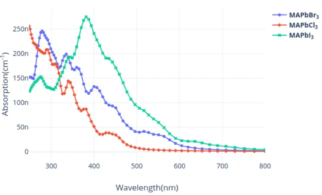
Band gap engineering
In addition to impressive high efficiency and low-cost fabrication, the major attractive feature is band gap tuning. This bandgap tuning is very useful for the preparation of tandem stack solar cell design[41]. The bandgap can be raised by adding Cesium(Cs), but band widening can also be archived by adding bromine(Br) in low concentration[7]. The most familiar perovskite used in solar cells is CH3N H3P bI3(1.55eV) and
A+PbI3 H Cs FA MA FAMA NH4
Bandgap N.A 1.7 1.47 1.55 1.5 1.8
Table 1.6.2: Band gap of perovskites with variation based on A site cations.
F AP bI3(1.47eV) which have a low bandgap with high absorbance in the visible region.
Bandgap can also be tuned by temperature variation, this is very evident in F AP bI3
perovskite where it ranges from 1.47eV to 1.58eV when the temperature is decreased from 300k to 160K. The organic cations regulate the bandgap by changing the bond distance between metal and halide[41]. The bandgap is increased from 1.55eV to 2.6eV when iodine(I) halide is replaced by bromine(Br).
Too small A site in perovskites leads to instability by tilting of octahedral networks which can change the electronic properties which were evident in the HP bI3structure.
The formamidine is asymmetric molecular ions, produces the distortion of geometry, and provides a fundamental reason for bandgap tuning[29]. While ABX3lattice, B is
the metal cation which directly influences the conduction band. The bandgap of the perovskites increases, when Pb is replaced by Tin(Sn) or germanium (Ge) the jump is bandgap is from 1.55eV to 1.7eV. In CH3N H3P bX3, the change in X site from I to Cl
Figure 1.6.3: UV–vis absorbance and band-gap values CH3N H3P bX3, X=I,Cl,Br.
1.6.2
Lead replacement in organometal halides
One of the attractive features of metal halide perovskite is the material properties can be tailored by changing the ionic composition of ABX3 lattices. This allows
us to identify some alternative metal while keeping the good optical and electrical properties of perovskite. Current research is focused on making the perovskite material non-toxic and stable for producing solar cells. Many alkaline and transition earth metals can achieve the divalent state and can be Incorporate in solution processing. The alternative mixed-metal perovskite composition Pb has been replaced by divalent metal species to form methylammonium mixed metal triiodide films, denoted by
M A(P b : BV )I3 where BV=[cobalt(Co), Copper(Cu), Iron(Fe), Manganese(Mn),
Magnesium(Mg), Nickel(Ni), Tin(Sn), and Zirconium(Zn)] [52]. Since research showed M AP bI3 has the highest defect tolerance then Co, Cu, Sn, and Zn[62].
One of the best suitable candidates to replace lead(Pb) is tin or germanium since it shows the very similar absorption as lead-based perovskite. But the use of tin or germanium is compromised due to the high oxidation instability [43]. A new wave of perovskite material has been developed in recent years with the ionic composition of
(a) Absorption peak of CsSnI3 (b) Absorption peak of CsP bI3
Figure 1.6.4: Comparative study of absorption peak of different perovskite with different metal anion.
Cs2AgBiI6, which is shown in figure 1.5.3a. Theoretical Density function theory(DFT)
calculation showed the bandgap close to 2.0-3.2 eV for the perovskite containing the lanthanide metal(LM) such as Eu, Dy, Tm, and Yb instead of lead-in (M A(P b :
LM )I3) compound. Due to this large bandgap lanthanide-based perovskite has a lot of
1.7
Fabrication method for perovskite solar cell
The main goal of solar cell fabrication is to have high power efficiency and large scale production. In the case of perovskite solar cell(PSCs) the major difficulty faced is to control the morphology of perovskite over a large area[38, 66]. PSC’s manufacturing technique is also important because it controls the layer roughness[53]. The salable technique used for PSC manufacturing is known as solution-based deposition and vapor-assisted deposition, which are further classified into subcategories as shown in figure 1.7.1.
Electron lifetime is depended directly on the type of film deposited, due to this the deposition can be done in one-step or two-step deposition. A typical one-step deposition is done using the mixture of both CH3N H3I and P bI3, while two-step
deposition is carried out using the separate layer deposition of both CH3N H3Iand P bI3
and results in a uniform defect free layer. Layers obtained by using one-step deposition contain voids which result in faster recombination[46]. While in two-step deposition the electron lifetime is higher than the one-step due to the better morphology control and the void-free layer.
Figure 1.7.1: Classification of fabrication method for perovskite solar cell
1.7.1
Solution Processing-Based Techniques
The solution processing based technique is the most widely used for the fabrication of Perovskite thin film. This can be classified into various techniques such as spin coating, spray coating, and dip coating. These techniques are illustrated as follows.
Spin coating technique
Spin coating is the cost-efficient and simplest solution-based technique for the uniform deposition of thin-film perovskite for solar cell application and this method can be used for fabrication of inverted (We will see in a later chapter) as well as regular PSC structures. Spin coating is followed by the baking step and results in the crystallized layers of the perovskite film. During baking a strong adhesion with the substrate and ensure the good bonding between the halogen cation and metal anion[45].Film thickness and quality can be controlled by spin speed, acceleration, and spin time. The main drawback with the spin coating is it is only applicable for producing small area solar cells, also slow processing and material wastage is high in the spin coating.
(a) Perovskite Spin coater (b) baking stage
Figure 1.7.2: Spin coating technique followed by baking process.
Spray Coating
Spray Coating is a solution based deposition used for the flexible solar cell due to its efficient and fast processing with less material loss. Unlike the Spin coating, spray coating can be used for large scale production. Spray coating is still in a development phase, but similar spray coating technique is in parallel development such as ink-jet printing[65]and slot die coating[44]. Despite this, the spray-coated thin film exhibits high thermal stability, better optoelectronic properties due to better charge transfer capability and high minority carrier lifetime[37]. This deposition technique is suitable for both planar and inverted perovskite solar cell devices[70]. Being so advantageous, there are some shortcomings such as difficulty in the deposition of highly homogeneous layers. This is caused due to the liquid atomization phenomenon. Liquid atomization
means when different sized droplets are sprayed randomly creates patches on drying, ultimately results in the increase in series resistance.
Figure 1.7.3: Approximation of thin-film deposition via spray coating[90]
Dip Coating or sol gel coating
Dip coating is also an efficient process for the production of perovskite thin film. In this method, the substrate is immersed in a solution containing the perovskite mix with the solvent. Once the thin film is developed then the substrate can be removed by evaporation[74]. The thin film thickness can be controlled by surface tension, gravitational force, the force of inertia[54]. The main advantage of using dip coating is low cost and layer thickness can be controlled precisely and the only drawback of dip coating is a slow process.
1.7.2
Vapour based technique
Vapour based technique also a dominating technique for the fabrication of thin-film perovskite for better film uniformity. Vapour deposition also results in the high crystalline structure and uniform thickness with good control over the thickness in the nanometer range. The main drawback is the small crystal size as compare to the solution-processed technique. highest PSC efficiency fabricated by vapor-based technique has reached an efficiency of 15.4%[67]. Vapor assisted deposition can be classified into two main categories, such as physical and chemical-based techniques as shown in figure1.7.1.
Figure 1.7.4: Vapor deposition of perovskite layers
Chemical vapour deposition (CVD)
It is a promising deposition technique for mass production of solar cells and pinhole-free perovskite thin film. CVD characteristic features like low material usage but difficult in controlling the deposition flux. CVD is optimized for the thin film perovskite by co-evaporation of two different precursors like CH3N H3I and P bI3, which are
heated, mixed, and transferred to substrate by carrier gas[92]. Thin-film developed using CVD has a larger grain size and long carrier lifetime.
Physical Vapor Deposition (PVD)
Physical vapor deposition (PVD), describes a variety of vacuum deposition methods which can be used to produce thin films and coatings. Various advantages of this technique are well-defined grain structure, high crystallization and reproducibility, and full surface coverage. This method avoids problems such as high reaction rate, impurities, improper heat treatment.
1.8
Challenges of Perovskite Solar Cell
The biggest issue with perovskite is long term stability, this degradation is caused by some external factors like moisture, light, and oxygen[9], also some internal factors such as degradation on heating[89].
Figure 1.8.1: The three pillars of successful commercial solar cells
1.8.1
Instability and degradation
Long-term instability is a very big issue with organometal halide based perovskite, despite good photon energy utilization like GaAs. But still, the stability can be improved by surface passivation[3] and by combining 2D perovskite with convectional 3D perovskite[100]. Degradation in perovskite solar cells can be caused due to two factors i.e extrinsic and intrinsic factors. These degradation parameters are discussed below in the context to M AP bI3.
Oxygen induced degradation
An important factor in the operation of the device is, it should be stable in the air without any encapsulation. Studies found oxygen cause the rapid degradation in
M AP bI3 perovskite thin film[16]. In an oxygen-rich environment, the deposited
is not true for the layer.
Since in the first generation PSCs used T iO2as an electron transport layer, since T iO2
is a dielectric material but it can be made as an n-type semiconductor by primarily introducing oxygen vacancies and interstitial defects during sputter deposition. Under the UV illumination these oxygen valencies a released and react with the perovskite active layer and create deep level defects and act as a recombination site.
Moisture induced degradation
Humidity is another degradation parameter when present during the manufacturing process readily degrade the perovskite thin film. The rate of deterioration is high when humidity combines with high temperature or electric field[80]. Since the organic cation in perovskite is hygroscopic(reactive to water molecule) in nature and form a week hydrogen bond with the cation which ultimately reduces the structural stability in M AP bI3 perovskite[24]. It also triggers the chain of the reaction shown below[24].
CH3NH3PbI3+H2O←−→ CH3NH3PbI3(Aqueous) + PbI2 (1.2) CH3NH3PbI3(Aqueous)←−→ CH3NH2(Methylamine) + HI(HydroiodicAcid) (1.3) O2+4 HI(HydroiodicAcid)←−→ 2 I2(Iodine) + 2 H2O (1.4)
UV light and temperature
Elevated temperature also causes degradation in PSCs, this degradation is seen in both M AP bI3 and M AP bCl3 based perovskite. Under high temperature and UV
radiation cause the M AP bI3 to degrade to P bI2 as as show in equation 1.2. Due to this
problem formamidinium lead iodide(F AP bI3) perovskite are used due to there better
photostability. The additional effect is seen in T iO2perovskite due to there instability
under UV radiation, this problem can be countered by the use of tin oxide(SnO2) as an
1.8.2
Methods of Increasing Stability and degradation
Cation mixing
The main cause of perovskite instability is caused due to the hygroscopic nature of organic cation, like M AP bI3, F AP bI3. Since the organic cation has a very little impact
on band structure and electrical properties. The main role is to balance the charge in the crystal but the size of the cation has a noticeable effect on the lattice structure. The bond between the anion and halide determines the bandgap and stability of perovskite[25]. Therefore, by varying the ratios of A-cations in the precursor, lattice qualities can be tuned/altered. Cation-A used in perovskite structure by tolerance factor (t):
t = √ ra+ ri
2(rP B+ i)
(1.5) Where riis the ionic radii, rAis the radius of the cation, and rP bis the radius of the lead molecule.
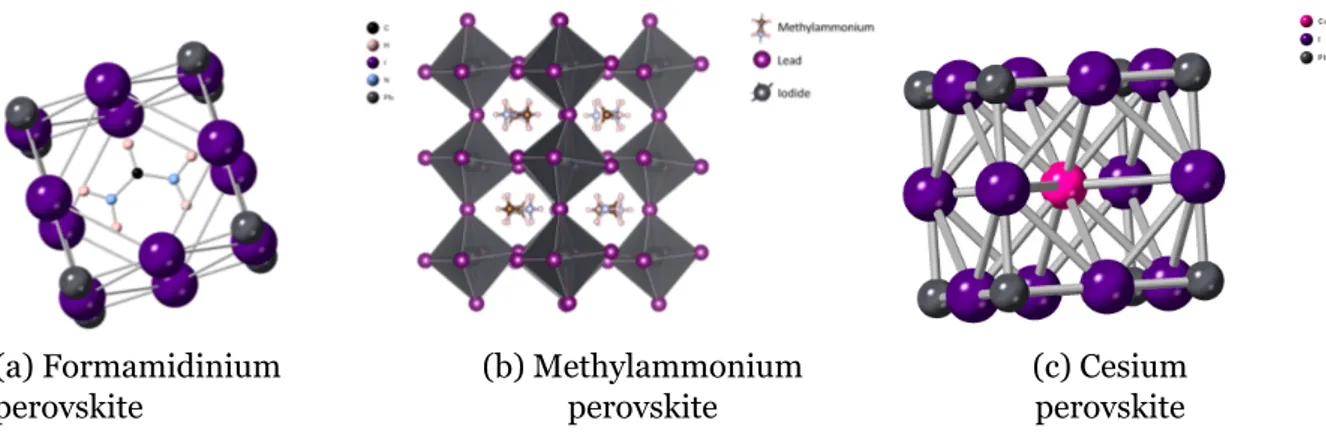
Cation size in lead halide perovskite results in distortion and tilting[62]. If the
(a) Formamidinium perovskite (b) Methylammonium perovskite (c) Cesium perovskite
Figure 1.8.2: Ball and stick models showing A-cation candidates used in perovskites.
tolerance factor is 1, then this produces a cubic perovskite structure. However, if the tolerance value falls between 0.7 and 0.9, then the tetragonal or orthorhombic phases can be induced. Formamidinium (FA) is an alternative to methylammonium, due to the high tolerance factor and existence of non-perovskite hexagonal phase at room temperature and limits the stability of the device, but perovskite phase can be recovered by heating. By combining MA and FA cations, a tolerance factor of almost 1 is reached[61].
Halide mixing
Another stoichiometric change to improve the solar cell stability is replacing iodine with other halide elements like chlorine or bromine since perovskite crystal is most stable in pseudo-cubic state i.e between cubic and tetragonal. The size of bromine and chlorine have a very different size then iodine, which results in a different lattice structure. By varying the ratios of these halides, band structure and stability can be changed[40].
Encapsulation
Figure 1.8.3: UV-curable epoxy applied to a perovskite solar cell and then sealed with a glass cover slip[78].
The method above discussed are intrinsic but the stability can be improved by an external technique like encapsulation. Encapsulation provides the best protection against external degradation catalysts, such as ambient moisture and UV light. A common method of encapsulation is to encompass the cell in a UV-curable epoxy resin, followed by a glass cover slip[78].
Thin-film perovskite photovoltaics
and SCAPS 1D
2.1
P-i-N junction
A variation of the p-n junction is the p-i-n junction, where a layer of semiconductor is left undoped between p and n-type semiconductors. The same built-in bias is established as P-n junction with the same doping levels, but the electrical field is extended over a wide region as shown in figure 2.1.1. This design is preferred in materials where the minority carrier diffusion lengths are short, and photo-generated carriers in p or n layers are unlikely to contribute to the photocurrent. Carriers that are generated in i-region are driven towards the contacts by the electrical field and carrier lifetime is relatively higher than the p-n junction. some of the disadvantages of p-i-n design are:
• The i region has poor conductivity and increases the series resistance in the solar cell.
• More recombination within the i region at forward biased condition, where electron and hole population is similar.
• Charged impurities may cause the electric field to fall zero within the intrinsic region.
The thickness of the i region should be optimized for the maximum current generation. Although more light is absorbed in a thicker region, charge defects reduce the electric
(a)
(b)
Figure 2.1.1: (a)Band profile of p,i,n-type semiconductor in isolation.(b) Band profile of p-i-n junction in equilibrium
field across the i region, and at some thickness, the width of the i region will exceed the space charge width as shown in figure2.1.2. The remaining, neutral part of the i region is a ”dead layer” and does not contribute to the photo-current. This design is preferred in materials where the minority carrier diffusion lengths are short, and photo-generated carriers in p or n layers are unlikely to contribute to the photocurrent. Carriers that are generated in i-region are driven towards the contacts by the electrical field and carrier lifetime is relatively higher than the p-n junction. The perovskite solar cell should be designed so that the depletion width is greater than the thickness of the i region at operating bias. In practice the i region thickness to around 0.5µm.
2.2
p-i-n solar cell physics
The first approximation is, the depletion approximation can be used to calculate the current-voltage characteristic of a p-i-n junction solar cell. We will consider a structure with p,i, and n layer with a thickness of xp, xn, and xi. Set x=0 at p-i interface and p, n-type have the doping density Naand Ndwhile i layer has background doping of Nidue to the charged impurity from n-type. The doping level of p and n layer is very high then
Figure 2.1.2: Electric field dropping across i layer with background impurities. The dashed line shows the electric field distribution at the point where the i region is just depleted as this line doesn’t end near n-type due to asymmetrical thickness of P and n layer.
the intrinsic region which results in the depletion width within the p and n regions are very small, so it can be neglected. In perovskite thin-film, background doping is low, results in the space charge region equal to the i-layer thickness.
Figure 2.2.1: Layer width of p-i-n junction structure.
The total current density(J) in given by the sum of jnand jpfor a p-n junction while in p-i-n junction it is given by:
Where JScris the current density from the i layer and each of the three contributes to give a particular bias V and generation rate (G). we have chosen the sign convention such that total current J is positive since current is flowing from p to n through the external circuit and makes the photocurrent as positive.
In perovskite solar cells the electron and hole transport layer(ELT, HLT) thickness is thin as compared to the active perovskite layer so approximation can be made that all recombination occurs in perovskite intrinsic layer. From the condition mentioned we only need to consider the photocurrent and dark current from the perovskite intrinsic layer. The net current density of perovskite solar cell will be:
J (V ) = JSC − Jdark(V ) (2.2) For p-i-n structure, the dark current is given is given by:
Jdark(V ) = √qnixi τnτp 2sinh(2kTqV ) q(Vbi−V ) kT ζ (2.3)
The above equation is a sah-Noyce-Shockley approximation, where factor ζ tends to π
2 for sufficiently large forward bias. τn, τp refer to the carrier lifetime in undoped
perovskite layer.ni, xi, V, Vbi refer as i-layer doping density, distance from junction, built-in voltage. The approximation is only valid for the intrinsic layer has a low background doping.
Photo-generated current in the perovskite intrinsic layer is given by:
JSC = ∫
q(1− R)be−αxi(1− e−αxi)dE (2.4)
Equation 2.4 is valid for the good carrier transport in the intrinsic region While in perovskite solar cell has a carrier lifetime of 1µs[94] and high mobility. The total photo-generated current is shown in equation 2.4, but it also has some contribution of drift current in i-region due to the applied biased voltage. So the reduced net photocurrent will be given by:
JSC∗ = JSC(1−
x2
i
µτ (Vbi− V )
Where µτ is the average mobility lifetime for both the carrier type. In equation 2.5 it is assumed that electron and hole densities vary linearly with distance in perovskite layer and have independent carrier lifetime and uniform photo-generation. Then drift length is given by:
Li =
µτ (Vbi− V )
xi
(2.6)
High background doped perovskite
If the background doping in perovskite is high then at biased voltage is above the threshold voltage then the i region will not be completely depleted, in this situation depletion width will be given by:
xi ≥
2ϵs(Vbi− V )
qNi
(2.7)
For a symmetric junction as voltage is increased the built-in bias is split between p-i and i-n interface, so that in the case of n type background doping in the i region only is doped across the p-i depletion region and depletion width is decreased to equation2.8.
Vbi = kT q ln( NaNi n2 i ) (2.8) Wi = 2ϵs(Vpi− V ) qNi (2.9)
In this situation, the photocurrent will be reduced and get bias voltage dependant and photocurrent will decrease with increases in Voltage. For high Ni levels this effect appears as a slope in the plateau of the J-V curve and could be confused with shunt resistance.
2.3
Characteristic of photovoltaics
2.3.1
Quantum efficiency and photo-current
The photocurrent generated by a perovskite solar cell under illumination at a short circuit depends on the light incident. Quantum efficiency(QE) relates the photocurrent density (JS C) to the incident spectrum. Quantum efficiency QE(E), is the probability that an incident photon of energy (E) will deliver one electron to the external circuit.
JS C = q ∫
bs(E)QE(E)dE (2.10)
where bs(E)is the incident photon spectrum flux density, the number of photon energy ranges from E and E+dE which are incident on the unit area in unit time.
QE and spectrum can be given as function of either photon energy or wavelength(λ), since sometimes energy is convenient way to represent band gap etc. So the relationship between E and λ is given by:
E = hc
λ (2.11)
Where h is the plank’s constant and c is the speed of light. For easy conversion wavelength(λ) is also equal to 1240
eV .
2.3.2
Dark current and open-circuit voltage
When the load is present, the potential difference is developed between the terminal of the cell. This generated potential difference will give rise to current, which flows in the opposite direction to the photo-current and the net current is reduced from its short circuit value. This reverse current is called dark current(Idark) which flows in the device under the applied voltage in dark. Perovskite solar cells behave like a diode, a large current flow in forward bias than the reverse biased condition. For an ideal solar cell dark current density is given by:
Jdark(v) = J0(e
qV
Where J0is a constant and T is the temperature and kBis Boltzmann’s constant.
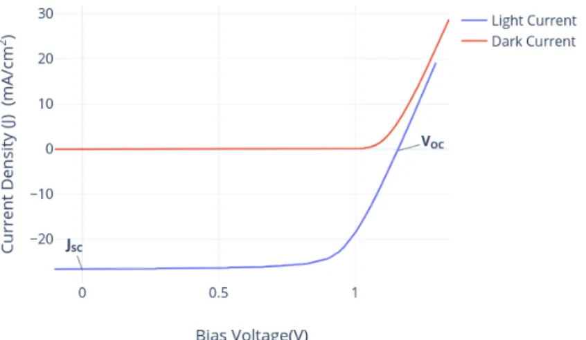
Figure 2.3.1: Current-voltage characteristic of perovskite solar cell in dark
Figure 2.3.2: Current-voltage characteristic of perovskite solar cell in dark with temperature sweep
From figure 2.3.2 is now evident that dark current value decreases with the decrease in temperature from the equation 2.12. We have followed the sign convection that photo-current is negative, make it easy for the electronics device analysis. The total photo-current density is given by an approximation while shifting the light current up by a constant amount and making it equal to dark current and marked the net current density as negative.
Figure 2.3.3: Current-voltage characteristic of perovskite solar cell in dark and light
When contacts are isolated, the potential difference is maximum and it is called as open circuit voltage(VO C). This is the exact point or equilibrium between the dark current and photo current exactly cancel each other.
VO C = kT q ln( JS C J0 + 1) (2.14)
From equation2.14, VO Cincreases logarithmic with the light intensity.
2.3.3
Efficiency
The power conversion efficiency of a semiconductor like a perovskite depends on the bandgap and incident spectrum. The theoretical maximum efficiency(ζ) is obtained by assuming the following:
• No photon with energy E smaller than EGis absorbed. • Each photon with energy E greater than EGis absorbed. • Each absorbed photon will give rise to an energy equal to EG.
From the above graph 2.3.4 we can conclude the maximum efficiency that perovskite solar cell can reach, range from 30% for formaldehyde perovskite to 27% for methyl-ammonium perovskite.
Figure 2.3.4: Maximum efficiency limit of solar cell
voltage(VO C)), in which cell produce power. Power density is given by J*V, and this value can reach to a maximum point which is know as maximum power point. As shown in figure 2.3.5.
F F = JmVm JS CVO C
(2.15)
Where FF stands for fill factor, and Vm, Jmstands for the voltage and current density at maximum power point, Vm
Jm know as the optimum load resistance. The efficiency(η)
of a solar cell is given by the power delivered at operating point as a fraction of incident light power density(Ps).
η = JmVm Ps
(2.16) Four quantities JS C, VO C, FF and η are the key parameters to characterise the performance of a solar cell. The standard testing condition for the solar cell is the Air mass 1.5 spectrum, with an incident power density of 1000 W m−2 and a temperature of 25°C.
Figure 2.3.5: Maximum power point calculation in solar cell.
Example calculation
From the above graph 2.3.5, we can find the Fill factor and efficiency of perovskite solar cell using equation 2.15, 2.16. The following can be deduced from figure 2.3.5,
Vm=0.894 v, Jm= 24.4 mA/cm−2, JS C= 26.6 mA/cm−2, VO C= 1.16 V. F F = 24.4X0.894 26.6X1.16 ∗ 100 = 70.69 (2.17) η = 24.4X0.894 100 ∗ 100 = 21.81% (2.18)
2.3.4
Parasitic resistance
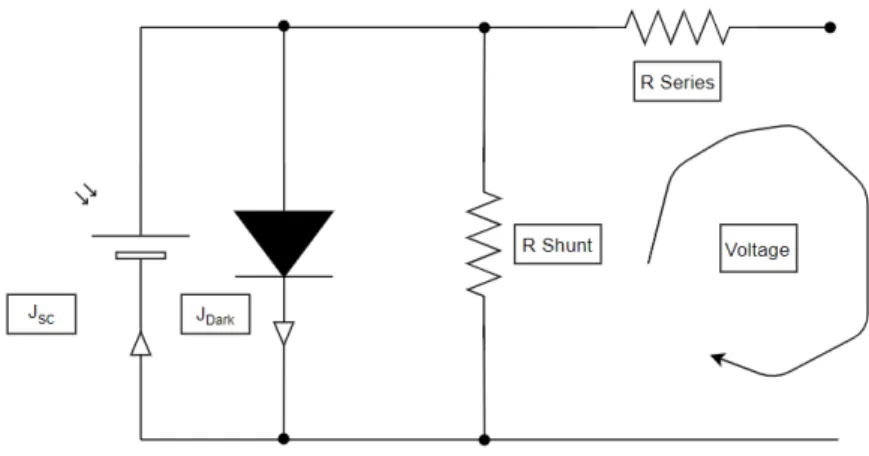
In an ideal solar cell there is no resistance, because the conductor used are consider to have no resistance, but in peorvskite solar cell contact are made up of gold or silver. Since gold or silver are consider best conductors but still have some resistance and results in the power dissipation, in thin film perovskite current leakage through the side due to the Small dimension of cell, also account for the power dissipation. These power dissipation can be represented as parasitic resistance in series and shunt in the ideal solar cell circuit as shown in figure 2.3.6.
Figure 2.3.6: Equivalent circuit of solar cell with series and shunt resistance
The series resistance is accounted for the solar cell material, here in this case is perovskite which typically has a series resistance of 5 Ω-10 Ω is observed when current is flowing through the device. Series resistance is problematic when there are high current density and concentrated light conditions. The shunt resistance rises due to the leakage current originate from the edge of the solar cell and between the contact of different polarities in the solar cell. For a good solar cell series resistance should be low as possible and shunt resistance to infinity. Parasitic resistance also reduces the fill factor as shown in figure 2.3.7. Due to the parasitic resistance the diode equation
(a) (b)
Figure 2.3.7: Effect of (a) decreasing series resistance and (b) increase in shunt resistance.
for total current density will become:
J =−JSC + J0(e
q(V +J ARs)
kT −1− V + J ARs
Rsh
2.3.5
Nonradiative Recombination
The open circuit voltage of solar cell is relatively lower then the radiative limits, which implies that there exist some nonradiative recombination mechanisms like Auger recombination[36] or Shockley–Read–Hall recombination caused by the recombination due to defects. In the real or practical device SRH recombination is much higher then other recombination mechanism. In total there are three recombination exist:
• Auger recombination
• Shockley–Read–Hall recombination
• Radiative recombination
Radiative recombination is caused due to the excess energy transferred to a photon by the recombination of electron and hole. In Auger recombination the excess energy is utilise to accelerate a third carrier which emit the photon by thermalization. In Shockley–Read–Hall recombination excess energy is also transferred to phonons and results in high lattice temperature.
Since the perovskite is microcrystalline which makes them far from the defect-free condition. Here, the most important recombination mechanism is recombination via Shockley–Read–Hall recombination due to sub-bandgap defects. These defect states can be, due to dangling bonds or defects arising from the material disorders. The recombination rate from Shockley–Read–Hall statistics is
R = np− n
2
i
(n + p)τ (2.20)
where τ is the lifetime of the charge carrier. This lifetime depends on the density of NT of defects states and the capture cross-section σ, and the thermal velocity vth.
![Figure 1.1.2: 90% of the city of Rotterdam lies below sea level, leaving many residential areas vulnerable to a rising ocean.[49]](https://thumb-eu.123doks.com/thumbv2/5doknet/3288953.21922/20.892.110.785.115.564/figure-rotterdam-level-leaving-residential-areas-vulnerable-rising.webp)