Design of a solar cell emulator
Academic year 2019-2020
Master of Science in Electrical Engineering - main subject Electronic Circuits and Systems Master's dissertation submitted in order to obtain the academic degree of
Supervisor: Dr. ir. Pieter Bauwens
Student number: 01405919
Design of a solar cell emulator
Academic year 2019-2020
Master of Science in Electrical Engineering - main subject Electronic Circuits and Systems Master's dissertation submitted in order to obtain the academic degree of
Supervisor: Dr. ir. Pieter Bauwens
Student number: 01405919
Declaration
The author gives permission to make this master dissertation available for consultation and to copy parts of this master dissertation for personal use. In all cases of other use, the copyright terms have to be respected, in particular with regard to the obligation to state explicitly the source when quoting results from this master dissertation.
Acknowledgements
First and foremost, I would like to thank my promotor, dr. ir. Pieter Bauwens. He was always helpful whenever I got stuck with a problem. He also provided me with useful ideas and information, and stayed very supportive during the many ”I’m completely stuck”-moments. Next, I want to thank dr. ir Herbert De Pauw, for kindly helping me solve the problem with the switching converters that would not boot. His door was also always open for questions, when I didn’t see an immediate solution. Thank you very much Herbert! Next, I would like the members of the CMST-group that provided me with useful feedback during the intermediate presentation in February, I evaluated and incorporated their suggestions as much as possible during the remainder of the master thesis. I would also like to thank Pieter and Davy, my co-directors of the BENDER Makerspace (FabLab Klein-Brabant) for listening to my endless whining about ongoing issues, while providing useful feedback and ideas. Lastly, I’d also like to thank my family for their patience and encouragement during this master thesis.
Hendrik Spildooren 31 May 2020
Abstract
This master thesis discusses the design of a solar cell emulator. This research was carried out at the Center for Microsystems Technology (CMST) at Ghent University under the supervison of dr. ir. Pieter Bauwens (thesis supervisor) and dr. ir. Herbert De Pauw.
Partial shadowing on solar cell installations is still a big problem. Such a shadow condition wastes available solar power, deteriorating the lifetime of the panels in the meantime. Another important factor is that the theoretical maximum efficiency limits are getting reached. This lead to extensive research in the domain of solving partial shadowing problems to boost the overall efficiency of a solar cell installation. One novel concept are the so-called ’Smart Reconfigurable PV’ (SRPV) panels [1], [2]. These panels can be configured to boost the output power (compared to the original case)if the solar panel is only partially illuminated. These panels consist of multiple switches and converters to dynamically reconfigure the panel in case of a shadow event. The issue is that the optimum conditions for (dis)connecting certain cells depend on the specific type of shadow condition. As testing these individual conditions on actual solar panels would be very cumbersome, the need arises for a solar cell emulator. This circuit should be able to behave exactly the same as a solar cell, while making it possible to mimic shadow conditions on the emulated cell. To this extent, a prototype PCB was fabricated and tested in order to evaluate the behaviour of a single element solar cell. After testing a single cell, the series and parallel connection of individual cells was investigated. These results were combined into useful IV-curves to produce a benchmark of the solar cell emulator. The design considerations and conclusions of these experimets are listed in this thesis dissertation.
Design of a solar cell emulator
Hendrik Spildooren
Supervisors: dr. ir. Pieter Bauwens, dr. ir. Herbert De Pauw
Abstract—Partial shadowing on solar cell installations is still a big problem. Such a shadow condition wastes available solar power, deteriorating the lifetime of the panels in the meantime. Another important factor is that the theoretical maximum effi-ciency limits are getting reached. This lead to extensive research in the domain of solving partial shadowing problems to boost the overall efficiency of a solar cell installation. One novel concept are the so-called ’Smart Reconfigurable PV’ (SRPV) panels [1], [2]. These panels can be configured to boost the output power (compared to the original case)if the solar panel is only partially illuminated. These panels consist of multiple switches and converters to dynamically reconfigure the panel in case of a shadow event. The issue is that the optimum conditions for (dis)connecting certain cells depend on the specific type of shadow condition. As testing these individual conditions on actual solar panels would be very cumbersome, the need arises for a solar cell emulator. This circuit should be able to behave exactly the same as a solar cell, while making it possible to mimic shadow conditions on the emulated cell. To this extent, a prototype PCB was fabricated and tested in order to evaluate the behaviour of a single element solar cell. After testing a single cell, the series and parallel connection of individual cells was investigated. These results were combined into useful IV-curves to produce a benchmark of the solar cell emulator. The design considerations and conclusions of these experimets are listed in this extended abstract.
Index Terms—solar cell emulator, smart reconfigurable photo-voltaic panels
I. INTRODUCTION
A solar cell emulator, based on a mixed-signal approach was designed. This mixed signal technique requires a digital component that stores the cell’s IV-curve. This IV-curve would then be applied to an analog output stage to produce the desired output voltage and current.
II. REQUIREMENTS
Such a mixed-signal solar cell emulator comes with a couple of requirements.
• Galvanic isolation between different cells. As cells need
to be connected in different arrangements, each cell need to be isolated from each other cell. This comes with a couple of design problems (such as isolated power supplies, isolated communication, etc.).
• 10 Acurrent capability. [2] and [1] mention a maximum
current capability of 10 A. This counts as another design constraint.
• Capabilities to dissipate power. The series and parallel
interconnection of cells requires the individual cells to be
able to dissipate power in conditions of partial shadowing. This makes for a required capability to dissipate power.
• Power source. The emulator should preferably be fed by
a single ’power brick’.
• Interconnection system. Different cells should
prefer-able be connected in an easy interconnection system, removing the hassle of running wires, screwing them in connectors, etc.
• Maximum current capability. As a parallel connection
of series cell strings is chosen, the parallel connection sums the individual output currents. To impose a design limit on this, a maximum of 4 parallel connected cells is allowed. This makes for a minimum current handling capability of 40 A.
III. CHOOSING THE DIFFERENT COMPONENTS FOR THE
SOLAR CELL EMULATOR
These requirements can be translated to an actual circuit. These requirements are:
• Main isolated power supply to provide output power.
This power supply should be able to provide the large amounts of output current at low output voltages. It should also be galvanically isolated. To this extent, the ADP1074 of Analog Devices was selected. This converter has a forward topology.
• Auxiliary isolated power supply. Next to the main
supply, a second isolated 5 V supply is needed to provide power to the microcontroller, the ADP1074’s secondary side, the analog circuitry supplies, the current sensors, etc.
• Power supply for driving additional analog circuitry.
As mentioned, analog circuitry is needed to drive the output stage and to provide feedback to the ADP1074. This was established by Texas Instrument’s LMC7660. In a first stage, the 5 V is boosted to a 9 V. In a second stage, this is boosted to 17 V and inverted to −9 V.
• Output stage. An output stage is designed to be able to
produce positive and negative output voltages (to be able to act as a generator and as a load). This output stage is steered by an analog driver, coming from a singe PWM output of the microcontroller.
• Microcontroller. The microcontroller should do a lot of
different things. It need to be fast, have a decent accuracy, be able to provide output under the form of a PWM output
or a DAC output and should have the necessary I2C
-interfaces. To this extend, the STM32F103C8T6 wast chosen.
• Output current and voltage sensing. Another
require-ment for a functional emulator is the measurerequire-ment of the vital parameters of the cell. It should be able to measure the output voltage and current. The first one is measured directly by the microcontroller by means of a voltage divider. The second one is performed by Texas Instrument’s INA219.
• Isolation between different cells. A final component is
the isolation between the different individual emulators. Ignoring this would break the isolation barrier. As such, this component is required in the design. This component was chosen to be
textitTexas Instrument’s ISO1040.
IV. DESIGN OF THEPCB
The assembled PCB is depicted in figure 1.
Fig. 1. Assembled single cell emulator.
V. TESTING AND RESULTS
Figure 2 depicts the obtained IV-curve of the single cell solar emulator for a 10 A short-circuit current.
-4000 -2000 0 2000 4000 6000 8000 10000 12000 -100 0 100 200 300 400 500 600 700 800 Cu rr en t [ m A] Voltage [mV]
IV-curve single cell (10A version)
Programmed IV-pairs Measured IV-pairs
Fig. 2. Example IV-curve obtained from the single solar cell. In this example, a short-circuit IV-curve current of 10 A was applied.
This single cell functionality is actually very good. As such, the interconnection of different single cells can be evaluated.
Fig. 3. Assembled series string of two cells.
Fig. 4. Assembled parallel connection of two cells.
To this extent, IV-curves of the series and parallel connection were tried to be obtained.
The problem is that the functionality at smaller load resistors could not be guaranteed. The ability to dissipate power was however verified to be working.
VI. CONCLUSION
This document demonstrates the working of a mixed-signal approach of a solar cell emulator. Some useful data was obtained for a single cell emulator. The interconnections of individual cells however should be further investigated.
REFERENCES
[1] P. Bauwens and J. Doutreloigne, “Switch for the optimization of module power by reconfiguration of all strings (SOMBRA): an insulated inte-grated switch for a reconfigurable solar panel,” ENERGIES, 2019. [2] P. Bauwens, J. Govaerts, M. Baka, F. Catthoor, K. Baert, G. Van den
Broeck, H. Goverde, D. Anagnostos, J. Doutreloigne, and J. Poortmans, “Reconfigurable topologies for smarter PV modules: simulation, evalua-tion and implementaevalua-tion,” in 32nd EU PVSEC, Proceedings, pp. 61–65, 2016.
Contents
Declaration Acknowledgements Abstract Extended abstract 1 Problem setting 12 Solar cell theory 3
2.1 Electrical model . . . 3
2.2 Simplified IV-curve . . . 4
2.3 Extended IV-curve . . . 6
2.3.1 ’Beyond’ constant current . . . 7
2.3.2 ’Beyond’ constant voltage . . . 7
2.4 Connection of multiple solar cells . . . 7
2.4.1 Series connection with even shadowing . . . 8
2.4.2 Series connection with partial shadowing . . . 9
2.4.3 Parallel connection with even shadowing . . . 10
2.4.4 Parallel connection with partial shadowing . . . 11
3 Boundary conditions & requirement list 13 4 Proposed solutions 15 4.1 Fully analog solution . . . 15
4.2 Mixed-signal approach . . . 16
5 Simulating different solar cells 18 6 Switching DC-DC converters theory 19 6.1 Non-isolated switching converter topologies . . . 19
6.1.1 Buck converter . . . 19
6.1.2 Boost converter . . . 20
6.1.3 Buck-boost converter . . . 20
6.2 Galvanically isolated switching converter topologies . . . 21
6.2.2 Forward converter . . . 22
7 First prototype 23 7.1 Aim of the first prototype . . . 23
7.2 Subdividing the system in multiple subsystems . . . 23
7.3 Galvanically isolated switching controller) . . . 23
7.4 Galvanically isolated low power supply . . . 26
7.5 Power supply to drive the analog circuitry . . . 27
7.6 Output stage . . . 28
7.7 Microcontroller . . . 29
7.8 Measuring the output current . . . 30
7.9 Isolated communication between different solar cell emulators . . . 31
7.10 Evaluation of the prototype . . . 31
8 Second prototype 33 8.1 Aim of the second prototype . . . 33
8.2 Design of the second prototype . . . 33
8.2.1 Modularity . . . 33
8.2.2 Current handling capabilities . . . 34
8.3 Firmware for the second prototype . . . 36
8.3.1 Single cell . . . 36
8.4 Evaluation of the second prototype: solved problems . . . 38
8.4.1 Hardware errata . . . 38
8.4.2 Loading of the charge pumps . . . 40
8.4.3 The ADP1074 could not be regulated . . . 41
8.4.4 The current sensor could not be found on the I2C bus . . . . 41
8.4.5 The second I2C interface cannot be used with the current sensor . . . . 41
8.4.6 The current sensor library returns invalid values . . . 41
8.4.7 The output voltage (and current) ripple is quite high . . . 42
8.4.8 The first I2C interface’s pins cannot be swapped, while this should be possible . . 43
8.4.9 ADP1074 not able to reach the maximum 10 A load . . . 44
8.4.10 Inability to dissipate power . . . 44
8.5 Evaluation of the second prototype: benchmarking the solar emulator . . . 45
8.5.1 Single cell emulator . . . 45
8.5.2 Series and parallel combination of cells . . . 46
8.6 Evaluation of the prototype: possible improvements . . . 48
8.6.1 Solve the issue with the voltage and current imbalance in series or parallel connected circuits . . . 48
8.6.2 Investigate the power dissipating capabilities . . . 49
8.6.3 Investigate the abilities to obtain higher cell voltages and currents . . . 49
8.6.4 Verify the correctness of the mismatch between different cells . . . 49
9 Future work 52 9.1 Investigate the series and parallel connection problems . . . 52
Bibliography 54
A IV-curve MATLAB simulation 55
B Schematics, layout and bill of materials of the second prototype 58
Chapter 1
Problem setting
Solar panels have gained huge interest over the last years. As the theoretical limits of converting solar power into electrical power are being reached, efficiency improvements are getting more focused towards other parts in the power generation cycle. One of them is partial shadowing. A solar panel (or module) typically consists of multiple individual single cells connected in a specific arrangement. It is this arrange-ment could possibly lead to losses, especially when only part of the photovoltaic installation is covered by shadow. In the past, this was solved using passive bypass and protection diodes [3]. They made sure no individual cells got damaged if such a situation would occur. But apart from protecting the cells, this method still wastes a lot of available power. This is why recent research started looking into a more intelligent solar panel, a so-called Smart Reconfigurable PV (SRPV) panel [1], [2]. Such a panel consists of multiple switches to reconfigure the individual solar cells dynamically within a panel. For example, the shadowed cells can be separated from the illuminated ones. This dynamic reconfiguration is combined with voltage converters (buck-boost converters) to create equal currents or voltages. As such, the power of the ’good’ (normal solar irradiation) cells is not wasted in the ’bad’ (shadowed, less solar irradiation) cells. On top of that, the lower output power of the ’bad’ cells is also used to deliver power by boosting it’s output voltage (or bucking the output voltage of the ’good’ cells). This makes the system potentially able to deliver a higher efficiency during conditions of partial shadow compared to the case where the shadowed cells are passively bypassed.
The aim of this master thesis is to develop a solar cell emulator circuit. This circuit should be able to mimic a single solar cell. Alternatively, the options of scaling this up to a ’group of cells’ as mentioned in [1] should be kept open. One of these configurations delivers an open-circuit voltage of 7.2 V, while delivering a 5 A current when shorted. The other configuration delivers 3.6 V without load and 10 A when shorted out. Preferably, these options are incorporated in the design. For the sake of simplicity however, in the continuation of this thesis, these configurations will be treated as a single cell. Another requirement is that these emulators should be fed by a ’power brick’ (figure 1.1).
The goal of this emulator is to be used in future research to emulate different shadow conditions, in different solar cell arrangements. This information could be used to evaluate the additional power saving (or loss). by implementing these switches and converters. Adding them will always introduces additional losses to the system so it is important to have an idea on how many switches and converters account for
Figure 1.1: Power brick.
how much efficiency improvement.
This dissertation starts with a general explanation on the electrical models that will be used and the different types of solar cell interconnections. This is followed by the translation of these conditions in a requirements list. After this, the possible solutions to solve this problem are given. This is followed by a small piece of theory on switching converters as they will be used frequently throughout the project. Next is the first prototype of the emulator in which the different components are tested. This precedes the second prototype, which is a more permanent version, on which the measurements were done. Lastly, some future work ends this dissertation.
Chapter 2
Solar cell theory
The purpose of this master thesis is not to explain the solar cell theory. However, the following part explains this cumbersome theory in a more simplified form, from an electrical point of view.
2.1
Electrical model
A single solar cell can be approximated by the electrical model in figure 2.1 ([3].
I
D
Rsh
Rs
Figure 2.1: Electrical model of a single solar cell. This model consist of 4 main components:
• Silicon pn-junction, modeled by a diode. In it’s most simple form, the solar cell is a (silicon) pn-junction that is capable of delivering a certain amount of current under certain conditions (see below for parameters that have an influence on this current). This pn-junction can be modeled as a regular diode. This diode applies to a regular diode IV-characteristic (figure 2.2a).
• Constant current source. This current source is the result of multiple physical parameters of
the solar cell. One of the most important ones is the solar irradiance (unit W/m2). This expresses
the solar intensity (power) of the incoming light per unit area. A larger irradiance translates to a larger short-circuit current. After losing some of this power by going from optical power to
electrical power, this translates into a short-circuit current density ([3], short circuit current) (Jsc,
unit A/m2). This parameter is a figure of merit for how much (short-circuit) current per unit of
V(out) 0.0V 0.2V 0.4V 0.6V 0.8V 1.0V 0A 1A 2A 3A 4A 5A 6A I(D) --- C:\Users\hspildoo\Desktop\Draft3.raw ---
(a) Characteristic IV-curve of the diode.
V(out) 0mV 70mV 140mV 210mV 280mV 350mV 420mV 490mV 560mV 630mV 700mV 0.0A 0.6A 1.2A 1.8A 2.4A 3.0A 3.6A 4.2A 4.8A 5.4A 6.0A I(Iout) --- C:\Users\hspildoo\Desktop\Draft3.raw ---
(b) Parallel connection of a current source and diode.
Figure 2.2: Constructing the solar cell model
to a normal constant current source by multiplying this density with the cell area. One can easily verify that this constant current source makes for an upward shift in the diode characteristic. If the
output is shorted, the voltage across the diode will be 0 V, resulting in an output current of ISC.
Contrary to that, if the output is left open, the diode will conduct all the current from the source, producing a positive voltage across the output terminals (corresponding to the current from the diode characteristic). This voltage-current characteristic of the output is depicted in figure 2.2b. • Parasitic resistances. The model (as every physical system) also contains a couple of parasitic
resistances
– Shunt resistor. A low shunt resistance on the output makes for a leakage path for the current.
This leakage path makes that less current flows through the diode. The result is an output voltage that gets ’dragged down’. If the shunt resistor is very low, this resistive behaviour
dominates, lowering the open-circuit voltage VOC ([3], shunt resistor ). Preferably, one would
like this shunt resistance to be as high as possible. Some graphs of the effect of a shunt resistor are depicted in figure 2.3b. Note that the slope in constant current mode is defined by the (low) shunt resistance.
– Series resistor. Again, depending on the size of the series resistor, the effects on the
IV-characteristic are more (or less) pronounced. A moderate resistance shifts the ’knee’ of the curve a bit more left down ([3], series resistor ), while excessive series resistances drag down the short-circuit current considerable, changing the characteristic completely. An example is shown in figure 2.4. Note that the slope in constant voltage mode is defined by the (low) shunt resistance.Typically one would like this series resistance to be as low as possible to limit losses.
2.2
Simplified IV-curve
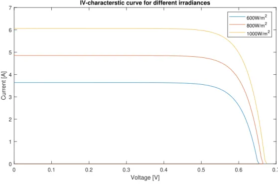
All the components of this model fit nicely together in the characteristic IV-curve. Some example curves for a solar cell with the following parameters is depicted in figure 2.5.
V(out) 0mV 70mV 140mV 210mV 280mV 350mV 420mV 490mV 560mV 630mV 700mV 0.0A 0.6A 1.2A 1.8A 2.4A 3.0A 3.6A 4.2A 4.8A 5.4A 6.0A I(Iout) --- C:\Users\hspildoo\Desktop\Draft3.raw ---
(a) Original characteristic, no shunt resistance.
V(out) 0mV 70mV 140mV 210mV 280mV 350mV 420mV 490mV 560mV 630mV 700mV 0.0A 0.6A 1.2A 1.8A 2.4A 3.0A 3.6A 4.2A 4.8A 5.4A 6.0A I(Iout) --- C:\Users\hspildoo\Desktop\Draft3.raw ---
(b) A 1 Ohm shunt resistance changes the charac-teristic. V(out) 0mV 6mV 12mV 18mV 24mV 30mV 36mV 42mV 48mV 54mV 60mV 0.0A 0.6A 1.2A 1.8A 2.4A 3.0A 3.6A 4.2A 4.8A 5.4A 6.0A I(Iout) --- C:\Users\hspildoo\Desktop\Draft3.raw ---
(c) A small shunt resistance (here 10 mOhm) dom-inates the characteristic completely.
Figure 2.3: Influence of the shunt resistance.
in the previous section, the reader can indeed verify that the four components of the model all have their influence on the IV-curve.
• In constant current mode (the area where the IV-curve looks ’flat’, the current is determined by the constant current source. It can be verified that the slope in this region is determined by the shunt resistance. As stated before, an increase in solar irradiance corresponds with an upwards shift of the IV-curve i.e. a larger short circuit current. The ’shape’ of the curve however stays more or less equal.
• At a certain voltage, the diode passes the threshold region, where it starts conducting current. This comes with the corresponding voltage drop across it. The output current starts to drop.
• At larger voltages, the solar cell is in constant voltage mode. The delivered current of course becomes zero if the load becomes open-circuited. The slope of the curve is now dependant on the series resistance.
In order to obtain power from the solar cell, it is important to note that the connected load will determine
the cell’s point of operation. A short circuit (0 Ohm load) will deliver a short-circuit current (ISC)
corresponding to 0 V, while an open circuit (∞ Ohm load) will put the open-circuit voltage (VOC) across
the terminals. One could easily verify that, for economical reasons, the solar cell will never be biased is these regions. To obtain the maximum available power, the cell will typically be biased in the ’knee’
V(out) 0mV 70mV 140mV 210mV 280mV 350mV 420mV 490mV 560mV 630mV 700mV 0.0A 0.6A 1.2A 1.8A 2.4A 3.0A 3.6A 4.2A 4.8A 5.4A 6.0A I(Iout) --- C:\Users\hspildoo\Desktop\Draft3.raw ---
(a) Original characteristic, no series resistance.
V(out) 0mV 80mV 160mV 240mV 320mV 400mV 480mV 560mV 640mV 720mV 0.0A 0.6A 1.2A 1.8A 2.4A 3.0A 3.6A 4.2A 4.8A 5.4A 6.0A I(Iout) --- C:\Users\hspildoo\Desktop\Draft3.raw ---
(b) A small series resistance (10 mOhm) changes the characteristic. V(out) 0mV 100mV 200mV 300mV 400mV 500mV 600mV 700mV 0.0A 0.1A 0.2A 0.3A 0.4A 0.5A 0.6A 0.7A 0.8A 0.9A 1.0A I(Iout) --- C:\Users\hspildoo\Desktop\Draft3.raw ---
(c) A large series resistance (here 1 Ohm) dominates the characteristic completely.
Figure 2.4: Influence of the series resistance.
of the IV-curve. Here, the product of the output voltage and the output current has the largest value. The maximum power point tracker (MPTT) that is part of the PV-installation, makes sure that the installation is delivering the maximum amount of available power.
2.3
Extended IV-curve
When connecting cells in series and parallel (e.g. into a solar module or panel), it is necessary to know what could possibly happen while doing so. Under normal conditions, the solar cell ends up in the known
first-quadrant IV-curve. The short circuit current ISC corresponds a 0 Ohm load, while VOC refers to an
open circuit or no attached load. At first glance, this region incorporates all physically possible loads. However, when differently shadowed cells are connected, there is the possibility in having a mismatch
([3], interconnection effects) in the cell’s ISC and VOC. These phenomena will be investigated in the
following subsections. These derivations will try to understand what happens ’beyond’ constant current regime (where the output voltage becomes negative) and what will happen ’beyond’ constant voltage regime. In order to do that, a simulation was made in LTspice, creating a more complete IV-curve. The model is depicted in figure 2.6a. This was performed by running a DC sweep across a load resistor. The parasitic resistors were given realistic values, and the diode was switched out for a diode that had a realistic breakdown and threshold voltage. The current sweep was plotted as a function of the output voltage of the cell. The results are given in figure 2.6b.
0 0.1 0.2 0.3 0.4 0.5 0.6 0.7 Voltage [V] 0 1 2 3 4 5 6 7 Current [A]
IV-characterstic curve for different irradiances
600W/m2
800W/m2
1000W/m2
Figure 2.5: MATLAB simulation (see chapter 5) of a solar cell using different values for the solar irradi-ance.
I
6
Rsh
100k
Rs
0.001
I1
D
OUT
.dc I1 -10 16
--- C:\Users\hspildoo\Desktop\Draft1.asc ---(a) Simulation model used for simulating the ex-tended IV-curve. V(OUT) -23V -20V -17V -14V -11V -8V -5V -2V 1V -10A -7A -4A -1A 2A 5A 8A 11A 14A I(I1) --- C:\Users\hspildoo\Desktop\Draft1.raw ---
(b) Simulation result of the extended IV-curve.
Figure 2.6: Simulation of the extended IV-curve.
2.3.1
’Beyond’ constant current
Beyond the constant current mode, the terminal voltage becomes negative. This voltage keeps getting more negative while the slope is still dictated by the shunt resistance. The pn-junction (diode) gets negatively biased. At a certain moment, this negative voltage makes the diode pass the reverse voltage breakdown barrier. The diode starts conducting exponentially more reverse current, permanently
dam-aging the junction. Mark that, beyond (0V, ISC) the solar cell is used as a load instead of a generator.
It thus dissipates power instead of delivering it.
2.3.2
’Beyond’ constant voltage
Beyond the constant voltage mode, the characteristic curve of the diode still holds. This means that exponentially more current will be conducted by the diode. This makes that the diode pulls additional current from outside the solar cell, acting again as a load instead of a generator.
2.4
Connection of multiple solar cells
The datasheet of a typical single solar cell [4] states that a single 12.5 cm x 12.5 cm solar cell can supply a short-circuit current of around 6 A and an open-circuit voltage of 0.7 V. This makes that the maximum available power from the solar cell equals more or less 3.5 W (disclaimer: this is depending on a lot of external factors, type of cell, efficiency, ...). It can be understood that it is not economically feasible to
encapsulate individual cells into protection against the elements. Moreover, consider resistive losses in the wiring, (and additional cost of this wiring). This is why single cells are typically arranged into a series-parallel configuration to form a solar module or panel. An example configuration is depicted in figure 2.7. This is a series connection of 36 single cells. However, other sizes (e.g. 60, 72, or even 96 ([3], module circuit design)) are possible, while other configurations are also available. The most common configuration is a parallel connection of series strings (however, the parallel connections are sometimes omitted, keeping only the series string). The problem is that the connection of individual solar cells into larger modules can introduce some problems.
Figure 2.7: An example series configuration of 36 individual cells, combined into a module. Note that one of the contacts is on the top of the cell, while the other one is on the bottom.
2.4.1
Series connection with even shadowing
Circuit theory dictates that the current flowing through a loop is the same, everywhere in the loop. This means that series cells, independently from the voltage across their terminals, all need to have the same current running through them. In the following thought-experiment, we assume perfectly equal conditions for two series-connected solar cells. The reader can verify that in this idealized case, the global IV-curve
has the same short-circuit current ISC, and the double open-circuit voltage VOC. This was verified by a
LTspice simulation, which is given in figure 2.8. Remark that the voltage and current axis have switched place as this makes it possible to plot them in the same window.
I1 6 Rsh1 100k Rs1 0.001 D1 I2 6 Rsh2 100k Rs2 0.001 D2 I3 OUT1 OUT2 .dc I3 0 6 --- C:\Users\hspildoo\Desktop\Draft1.asc ---
(a) Model used for simulating the series connection.
I(I3)
0.0A 0.6A 1.2A 1.8A 2.4A 3.0A 3.6A 4.2A 4.8A 5.4A 6.0A
0.0V 0.1V 0.2V 0.3V 0.4V 0.5V 0.6V 0.7V 0.8V 0.9V 1.0V 1.1V 1.2V 1.3V 1.4V 1.5V V(out2) V(n001)-V(n002) V(out1) --- C:\Users\hspildoo\Desktop\Draft1.raw ---
(b) Simulation result of the series connection.
2.4.2
Series connection with partial shadowing
While the simulations of the idealized case give convenient results, problems could appear when partial shadowing arises. Assume the same two cells, identical in physical construction, but one of them receives less solar irradiance (it is covered by shadow, e.g. due to a tree). As stated before, this can be modeled by lowering the value of the constant current source. Simulating this, results in figures 2.9a and 2.9b. Assume the short-circuit of the global IV-curve is calculated now. This results in the following:
• The short-circuit current is defined as the amount of current for which the terminal voltage equals 0 V.
• The current flowing through the loop is however limited by the ’weakest’ cell. This is however only an approximation as there is a very slight slope, dictated by the shunt resistance, but for now, the curve is approximated as being ’flat’.
• This means that, the ’stronger’ cell will be biased around a positive terminal voltage.
• In order to get 0 V at the terminals of the global system, the ’weak’ cell thus needs to be biased around a negative voltage. The weak cell is acting as a load, consuming part of the power generated in the ’good’ cell.
It can be verified that the negative voltage across the ’weak’ cell doesn’t always need to be the case. If the global curve is biased around a voltage that is large enough, this will not happen. However, the result of this calculation is that the solar cell arrangement produces less power than expected. On top of this, part of the generated power in the ’good’ cell gets dissipated in the ’bad’ cell. This can be verified in the LTspice simulation depicted in figure 2.9c. This graph simulates the power delivered by the different cells. It can be seen that, at short circuit, the first cell produces a positive output power, while the second cell ’produces’ a negative power. The first one is thus acting as a generator, while the second one is acting as a load. It should be no surprise that, if many cells would be connected in series, this could lead to a couple of disadvantages:
• The dissipated power in the ’bad’ cell heats up the cell. This could shorten the lifetime of the cell dramatically. This effect is called ’hot spot heating’ ([3], hot spot heating), referring to the one cell (spot) in the panel that is significantly hotter than the rest of the panel.
• The negative voltage across the shadowed cell could reach levels that surpass the reverse breakdown voltage of the pn-junction. This would permanently damage the cell, rendering the complete series string unusable.
Consider another following thought-experiment. A solar panel consists of 72 individual series connected
cells. Under a 1000 W/m2 irradiation, this translates to an approximate short-circuit current I
SC of 6 A
and an open-circuit voltage VOC of 0.7 V. Assume one single cell is shaded, reducing it’s constant current
to e.g. 1 A. The short-circuit current of panel is thus limited to 1 A. This biases the fully irradiated cells to approximately (0.6V, 1A), while short-circuiting the partially shadowed cell. If the panel itself would become short-circuited now, there would be 0 V across the output. As such, the voltage across
the shadowed cell is approximately equal to −(0.6V x72) = −42V . If this doesn’t kill the cell due to the
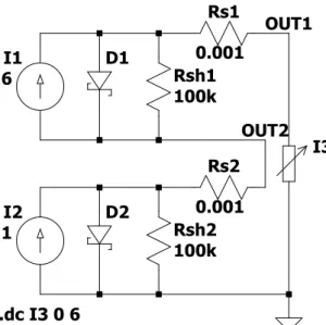
I1 6 Rsh1 100k Rs1 0.001 D1 I2 1 Rsh2 100k Rs2 0.001 D2 I3 OUT1 OUT2 .dc I3 0 6 --- C:\Users\hspildoo\Desktop\Draft1.asc ---
(a) Model used for simulating the partially shad-owed series connection.
I(I3)
0.0A 0.6A 1.2A 1.8A 2.4A 3.0A 3.6A 4.2A 4.8A 5.4A 6.0A
-2.00V -1.75V -1.50V -1.25V -1.00V -0.75V -0.50V -0.25V 0.00V 0.25V 0.50V 0.75V 1.00V 1.25V 1.50V 1.75V 2.00V V(out2) V(n001)-V(n002) V(out1) --- C:\Users\hspildoo\Desktop\Draft1.raw --- (b) IV-simulation result.
0.9995A 0.9996A 0.9997A 0.9998A 0.9999A 1.0000A 1.0001A 1.0002A 1.0003A 1.0004A 1.0005A -11V -10V -9V -8V -7V -6V -5V -4V -3V -2V -1V 0V 1V 2V 3V -11W -10W -9W -8W -7W -6W -5W -4W -3W -2W -1W 0W 1W 2W 3W
V(out1) (V(out1)-V(out2))*I(I3) V(out2)*I(I3)
--- C:\Users\hspildoo\Desktop\Draft1.raw ---
(c) Power simulation result (global IV-curve was added for reference).
Figure 2.9: Simulating the series connection of partially illuminated series cells.
cell. This will definitely destroy the cell, damaging the whole panel with it.
Currently, this hot spot heating and junction breakdown problem is solved by bypass diodes. Every so often couple of series cells, a diode is placed in parallel these cells. Typically, this is a (low threshold) Schottky diode. This bypass diode is connected antiparallelly with the series string. Suppose a shadowed string would become reverse biased at some point at a voltage larger than the threshold voltage of the diode. The diode starts conducting current, protecting the cell from possible damage, thus limiting losses. It should be noted that, while this is an easy solution, this still wastes a non-negligible amount of power. First of all, the diode still dissipates some power. Secondly, the shadowed cell might actually be able to produce power, if it would have been biased in another point of the IV-curve. This is why the dynamically reconfigurable photovoltaic panels were proposed as a possible solution [2], [1].
2.4.3
Parallel connection with even shadowing
For the parallel connection of solar cells, the same reasoning can made as with the series cell connection. If cells are connected in parallel, the voltage across all cells is the same, while the total output current is simply the sum of the individual output currents. This was verified by a LTspice simulation. The model
is depicted in figure 2.10a, while the results are displayed in figure 2.10b. Note that for the sake of being able to plot all graphs in the same window, the voltage is plotted on the horizontal axis again, while the current is located vertically.
I1 6 100k Rsh1 Rs1 0.001 D1 I2 6 100k Rsh2 Rs2 0.001 D2 I3 OUT .dc I3 0 12 --- C:\Users\hspildoo\Desktop\Draft1.asc ---
(a) Model used for simulating the parallel connec-tion. V(out) 0mV 100mV 200mV 300mV 400mV 500mV 600mV 700mV 0A 1A 2A 3A 4A 5A 6A 7A 8A 9A 10A 11A
12A -I(Rs1) -I(Rs2) I(I3)
--- C:\Users\hspildoo\Desktop\Draft1.raw ---
(b) Simulation result of the parallel connection.
Figure 2.10: Simulating the parallel connection of equally illuminated cells.
2.4.4
Parallel connection with partial shadowing
The same analogy with the series connection of cells could again be made. Contrary to the previous series analysis, possible problems could arise in the constant voltage regime. Shadowing one cell pulls
the IV-curve down, so the open circuit voltage VOC will be slightly less than the fully irradiated one.
This can be seen in figure 2.11b. Assume the objective is now to calculate the open-circuit voltage of the global IV-curve. The following reasoning could be made.
• The open-circuit voltage is defined as the terminal voltage for which the delivered current equals 0 A. This means that the current through one cell is exactly opposite to the current running through the other one.
• The next requirement is that the voltages across the cells are exactly the same.
• The same reasoning of a ’flat’ region could be made. Mark that the accuracy of this approximation depends on the slope of the graph, or the series resistance. This makes that the ’weak’ cell will ’dictate’ the behaviour. The ’good’ cell will thus be biased around the same voltage and a nonzero current.
• As a total current of 0 A is required, the ’weak’ cell thus needs to be biased around a negative current. The weak cell is acting as a load, consuming part of the power generated in the ’good’ cell. As mentioned in the third bullet, the ’flatness’ of the curve in the constant voltage region is typically not as steep as in constant current mode, but the operational principle stays the same. The system finds an equilibrium that will be somewhere in between the open-circuit voltage of the ’weaker’ cell and the open-circuit voltage of the ’stronger’ cell. This partial shadowing problem for parallel cells in constant current mode can result in damage, but is typically not as harmful as the series constant-current case. Some arguments that support this statement are listed below.
• The ’not-so-steep’ slope makes sure the ’weak’ cell will typically not be biased around a very large negative current. This limits the dissipated power in the cell.
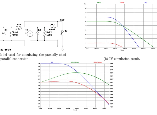
I1 6 100k Rsh1 Rs1 0.001 D1 I2 1 100k Rsh2 Rs2 0.001 D2 I3 OUT .dc I3 -10 10 --- C:\Users\hspildoo\Desktop\Parallel.asc ---
(a) Model used for simulating the partially shad-owed parallel connection.
V(out) 0mV 100mV 200mV 300mV 400mV 500mV 600mV 700mV 0A 1A 2A 3A 4A 5A 6A 7A 8A 9A
10A -I(Rs1) -I(Rs2) I(I3)
--- C:\Users\hspildoo\Desktop\Parallel.raw --- (b) IV-simulation result. V(out) 0mV 100mV 200mV 300mV 400mV 500mV 600mV 700mV -7A -6A -5A -4A -3A -2A -1A 0A 1A 2A 3A 4A 5A 6A 7A -4.8W -4.2W -3.6W -3.0W -2.4W -1.8W -1.2W -0.6W 0.0W 0.6W 1.2W 1.8W 2.4W 3.0W 3.6W
I(I3) -I(Rs1)*V(out) -I(Rs2)*V(out)
--- C:\Users\hspildoo\Desktop\Parallel.raw ---
(c) Power simulation result (global IV-curve was added for reference).
Figure 2.11: Simulating the parallel connection of partially illuminated series cells.
• The difference in open-circuit voltages between the cells is normally not that large, which results again in a limited power dissipation in the ’weaker’ cell.
• For this problem to arise, solar cells need to be connected in parallel. Most solar panels are however fully series connected or (more rare) parallel connections of series strings. If parallel connections are present, there are typically more cells in a series string, than there would be parallel strings in a panel (e.g. 6 strings of 12 cells). A worst-case scenario would be that one string completely gets covered, while the other strings are fully illuminated. This would mean that, with respect to the series case, one shadowed cell would be dissipating power coming from a smaller number of cells. This also limits the power possible power dissipation.
To conclude, the effect open-circuit voltage mismatch in a parallel connection possibly has a smaller effect on the proper operation of the solar panel than a short-circuit current mismatch in a series connection. As a side note, this effect is not negligible anymore when whole modules are connected in parallel. However, a rigorous study of this type of mismatch is out of the scope of this master thesis.
Chapter 3
Boundary conditions & requirement
list
From the solar cell theory, we can derive some boundary conditions for the solar cell emulator itself. These boundary conditions are chosen to simplify the circuit that will emulate the solar cell. These simplifications include the following.
• It is assumed that the solar cell can ’produce’ a negative output voltage. This means that the emulator needs to be able to function as a load. This loading however has some limits. The current during this case can be considered constant. This would mean that the power dissipation in the cell would grow linearly with the reverse voltage across the cell. The region of breakdown will however not be taken into account in the design. This will limit the cell’s inability to be able to dissipate lots of power (in the order of hundreds of Watts). The power dissipation capabilities in this design will be limited to a moderate power level (<10 W). If the power should exceed this level, the circuit should be able to protect (e.g. stop the increasing negative terminal voltage) itself from dissipating more power.
• A second constraint is that the cell’s capability of working in the fourth quadrant will be limited. This will relax the difficulties considerably. Otherwise, current would also need to be able to flow into the cell other than only out of the cell.
• A non-negotiable element of a solar cell is the fact that multiple cells can be put into series or parallel configurations, without limitations. This means that each cell needs to be isolated completely from each other cell. This will add complexity to the design as the cells cannot share a common (ground) connection. Galvanic isolation between all cells should thus be implemented, adding complexity to the design.
Next to these boundary conditions that are linked to the IV-curve of the solar cell, we further add some constraints to the circuit:
• Preferably, the solar cell configuration is fed from a single power supply (typically a power brick) with a moderate output voltage (12 V-36 V), able to provide a sufficient output power for the
emulator.
• To limit the complexity, the maximum allowable current through a single cell is fixed to 10 A. This sets a design limit to the switching power supply and the width of the PCB traces. This output current should be able to be maintained throughout the cell.
• Ideally, the cells can be connected in some kind of series-parallel form by means of a single connector system.
• The total current through cells that are connected in parallel may not exceed the 40 A limit. This sets a design constraint on the PCB track width of the interconnection (PCB’s). This makes for a maximum of 4 parallel strings of series cells.
Chapter 4
Proposed solutions
During the investigation of the possible solutions, two possible solutions came to mind. They’re briefly described below.
4.1
Fully analog solution
One possible solution is the fully analog implementation of a solar cell. In this approach, a constant current supply should be designed, connected to a diode, and parasitic resistances. The design would quite literally try to implement the electrical model of the solar cell. The advantage of this approach is that the implementation should be quite straightforward, the components are well determined. The main components this solution asks for are a constant current source, and some flexibility options to somehow ’change’ the characteristic of the diode and the parasitic resistances. A very simple adjustable constant current circuit is given in figure 4.1. This circuit works by forcing the desired voltage across a sensing
resistor. This makes for a current Vset/Rsensethrough the load. This constant current source would need
to be connected to a certain discrete diode. Adding flexibility would be not easy here, the diode is a discrete component with it’s own typical characteristics. Lastly, output resistors should be added to the circuit. V_SET MOSFET R_SENSE R_LOAD V_IN_ISOLATED --- C:\Users\hspildoo\Desktop\Draft3.asc ---
As mentioned before, the major drawback of this implementation is the lack of flexibility. The ideal case would be to implement a variable IV-curve. In this solution, the diode characteristic is fully fixed, which limits the freedom in the number of possible IV-curves.
4.2
Mixed-signal approach
Another approach could be the following. Suppose the desired IV-curve is stored in the memory of a digital component (here, assumed to be a microcontroller). If it would be possible to somehow apply this curve to an output stage, this digitally programmed curve is translated to the analog domain. This implementation also comes with a couple of problems. Together with the need for galvanic isolation between cells, there will be a lot of added complexity in this solution. Some examples of increased complexity include:
• Control loops. Possibly, extra control loops need to be introduced. For example to regulate additional supplies or the output stage. These control loops need to be stable, they need to be able to produce the correct voltage ranges, etc.
• Current and voltage monitoring. This is part of the mentioned control loop. The cell’s output voltage and current need to be monitored in order to let the microcontroller take the decision whether the output voltage needs to be increased or decreased.
• Communication between cells. This solution would possibly also need to be able to communi-cate between other cells and possibly also with some kind of ’master’ cell. Connecting the busses of all cells would break the isolation barrier between cells. Bus isolation would also be required in this solution.
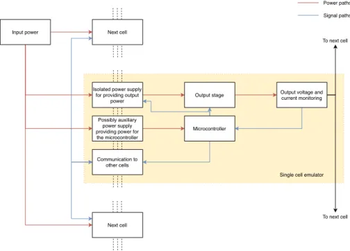
The reader can verify that this implementation would require a lot more careful thinking than the analog solution. However, this hassle comes at the additional freedom of the more ’adjustable’ and programmable IV-curves. A first overview of how a mixed-signal solar cell should look like is depicted in figure 4.2. Ultimately, the mixed signal solution was chosen over it’s analog counterpart. The main reasons for this were already given above. The possibility to be able to add ’any’ IV-curves in software, on the fly, made the ’mixed-signal’ approach more attractive than the ’analog’ solution.
Isolated power supply for providing output
power
Possibly auxiliary power supply providing power for the microcontroller Communication to other cells Microcontroller Output stage Input power Next cell ```` Next cell
Output voltage and current monitoring
To next cell To next cell
Single cell emulator Power paths Signal paths
Figure 4.2: First overview of how a mixed signal cell emulator could possibly look like. Note the dotted line, indicating the galvanic isolation.
Chapter 5
Simulating different solar cells
The mixed-signal solution asks for an IV-curve, programmed in software. There is thus a need for some data points or (voltage, current) pairs. As already shortly mentioned in the section 2.1, this was performed by modifying an existing IV-curve plotting script [5] that takes physical constants as depicted in subsection 2.1. This was adapted to output the current and voltage pairs as arrays, readable by the source code used to program the microcontroller. The complete simulation file is linked in appendix A. The parameters are used to solve the solar cell equation corresponding to the electrical model. This results in IV-curves, plotted in figure 5.1.
0 0.1 0.2 0.3 0.4 0.5 0.6 0.7 Voltage [V] 0 1 2 3 4 5 6 7 Current [A]
IV-characterstic curve for different irradiances
600W/m2 800W/m2 1000W/m2
Chapter 6
Switching DC-DC converters theory
The complete detailed study of switching converters is cumbersome and beyond the scope of this thesis. However, as these types of DC-DC converters get used throughout the whole design of the solar cell emulator, the most basic theory of operation is repeated here.
6.1
Non-isolated switching converter topologies
While not used in this thesis, the theory of operation of the non-isolated switching converters is explained here. The working principle can be extended to isolated topologies by replacing their current storing element (inductor) with a transformer. These non-isolated types of converters are typically chosen for their low complexity and high efficiency.
6.1.1
Buck converter
As the name implies, the buck converter transforms a higher input voltage into a lower output one. The circuit is depicted in figure 6.1a. The working principle can be derived as follows [6]. For the sake of simplicity, the most simple case, only ’constant conduction mode’, or CCM (the current through the inductor always remains larger than 0 A) is assumed. The circuit contains one switching element (MOSFET in this example). This switching element has two states, either ON or OFF. During the
ON-state, the inductor has a voltage across it that is equal to Vin− Vout (negative, as the input is larger
than the output), while diode D1 is reverse biased. The current running through the inductor is rising
and energy stores energy in the meantime. During the OFF-state, the diode becomes forward biased, the
voltage across the inductor is now equal to−Vout− VD1. The current through the inductor is decreasing.
If the assumption that the voltage drop across the diode can be neglected is made, an energy balance during the whole state can be computed. The amount of energy at the beginning of a cycle needs to be the same as at the end of the cycle. Imposing this, the output voltage can be computed. It turns out that
this output voltage vout is approximately equal to the duty cycle of the switch multiplied with the input
voltage Vin. The LTspice simulation in figure 6.1b confirms this working principle. The input voltage of
24 V turns into an output voltage of 12.8 V by using a 60% duty cycle. The slight difference is due to the (wrong) assumption of the 0 V voltage drop across the diode.
reaches 0 A at some point during the cycle). In that case, the OFF-state should be split up in two parts. This derivation (and the resulting formulas) are a bit more complicated, but they follow the same reasoning. VIN 24 VS PULSE(0 24 0 0 0 6u 10u) D C 220µ L 220µ RL 10 OUT .tran 0 100m 30m
(a) Schematic of a buck converter.
26.502ms0V 26.514ms 26.526ms 26.538ms 26.550ms 26.562ms 1V 2V 3V 4V 5V 6V 7V 8V 9V 10V 11V 12V 13V 14V 15V 1.00A 1.05A 1.10A 1.15A 1.20A 1.25A 1.30A 1.35A 1.40A 1.45A 1.50A V(out) -I(L) --- C:\Users\hspildoo\Desktop\Draft2.raw --- (b) Waveforms of the buck converter.
Figure 6.1: Simulating a buck converter.
6.1.2
Boost converter
A similar derivation can be made for a boost converter. This converter uses a lower input voltage to transform it to a higher output voltage. Schematically, this is depicted in figure 6.2a. Concerning the working principle, a fully analog reasoning could be made [6]. The result in constant conduction mode
turns out to be that VOU T = 1/(1− D), with D being the duty cycle. This behaviour was confirmed by
another LTspice simulation, which is given in figure 6.2b. The input voltage of 10 V turns into an output voltage of 28 V by using a 60% duty cycle. Theoretically, this should be 25 V, which is again close to the proposed solution. VIN 10 VS PULSE(0 10 0 0 0 6u 10u) D C 220µ L 220µ RL 100 OUT .tran 0 100m 30m --- C:\Users\hspildoo\Desktop\Boost.asc ---
(a) Schematic of a boost converter.
17.620ms0V 17.628ms 17.636ms 17.644ms 17.652ms 17.660ms 17.668ms 2V 4V 6V 8V 10V 12V 14V 16V 18V 20V 22V 24V 26V 28V 30V 0.64A 0.68A 0.72A 0.76A 0.80A 0.84A 0.88A 0.92A 0.96A 1.00A 1.04A 1.08A 1.12A 1.16A V(out) -I(L) --- C:\Users\hspildoo\Desktop\Boost.raw ---
(b) Waveforms of the boost converter.
Figure 6.2: Simulating a boost converter.
6.1.3
Buck-boost converter
Trivially, this is the combination of the previous two examples, it can either transform an input voltage into a lower output voltage or a higher output voltage. This topology is especially useful if the input voltage is not known on the beforehand (some examples include batteries, some energy harvesting appli-cations, a wide voltage range input, etc). This typically comes at the expense of a slightly worse efficiency.
Multiple topologies are possible. A first one is the so-called inverting topology. This uses a very similar setup as the buck and boost converters, but has an inverted output voltage. Another one is the ’four-way-switch’-topology [7]. This topology is actually a combination of the buck and boost topology into one circuit. This is done by introducing a second diode and switch to either one of the circuits. Alternatively, the diodes could also be replaced by switching elements, hence the name, ’four-way-switch’.
6.2
Galvanically isolated switching converter topologies
As stated before, the above topologies can typically be extended by replacing the inductor with a
trans-former. Their naming is also slightly different. W¨urth Elektronic has made a nice comparison table
that can be found here: http://www.we-online.biz/web/en/index.php/show/media/07_electronic_ components/news_1/blog/midcom_blog_photos/SMPSChart.pdf. The flyback and the forward con-verter are listed down below. Galvanically isolated topologies are typically harder to design and are less cost-effective than their non-isolated topologies. This is because instead of a single inductor, the topology needs a transformer. In order to keep the voltage source regulated, there is also the need for providing feedback from the secondary side to the primary side (typically done via an optocoupler).
6.2.1
Flyback converter
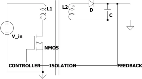
The flyback converter can be considered the isolated version of a buck-boost converter. If the ’dot’ on the transformer is chosen appropriately, the transformer can also be used to flip the sign of the inverted output voltage back to the ’normal’ positive output voltage. The flyback converter can thus be used to create either higher or lower output voltages from a given power supply. The transformer supplies the needed galvanic isolation between the primary and secondary side. These types of converters are typically used in cheap AC-DC power supplies (phone chargers, power supplies of TV’s, etc.). A typical configuration is shown in figure 6.3. Conversion from AC to DC is typically done by means of (full bridge) rectifier, followed by a large smoothing capacitor. This creates a high voltage DC supply, after which the DC-DC-conversion by means of a flyback convertor takes place. In this AC-DC applicatio, flyback converter is used here as a normal buck-boost doesn’t provide the life-saving isolation between the power grid and the electrical appliance’s output. If this wouldn’t have been the case, the output would be referenced directly to mains voltage, what would possibly lead to lethal incidents.
L1 L2
NMOS V_in
D
C
CONTROLLER ISOLATION FEEDBACK
--- C:\Users\hspildoo\Desktop\Draft5.asc ---
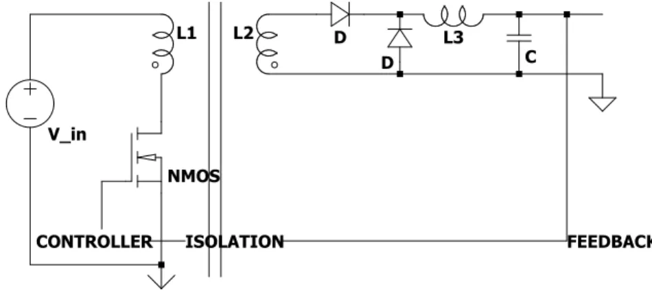
6.2.2
Forward converter
While the flyback converter was able to either buck or boost the input voltage, the forward converter can only be used to create an output voltage that is smaller than the input voltage. A typical example is depicted in figure 6.4. L1 L2 NMOS V_in D D L3 C
CONTROLLER ISOLATION FEEDBACK
--- C:\Users\hspildoo\Desktop\Draft5.asc ---
Chapter 7
First prototype
7.1
Aim of the first prototype
The aim of the first prototype is to evaluate the different building blocks, spotting possible problems early on in the design. From the translation of the mixed-signal solution and the requirement list depicted in chapter 3, the emulator got subdivided in the subsystems listed below.
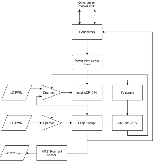
7.2
Subdividing the system in multiple subsystems
Multiple different subsystems make the design more manageable. The following subsystems can be distinguished. An overview (block diagram) of the solar cell emulator is depicted in figure 7.1.
• Galvanically isolated power supply to deliver the needed output power. • Output stage to drive the connected load from the main power supply.
• Isolated power supply to drive the secondary side analog components and logic (microcontroller, secondary side power, current sensors, etc.).
• Analog power supplies on the secondary side to drive the analog components (operational amplifiers to drive power stage and feedback stage).
• Galvanic isolation on the I2C bus that is used to connect all ’slave’ cells and possibly the ’master’
cell.
7.3
Galvanically isolated switching controller)
The isolated switching controller needed to meet certain requirements. It needed to be able to supply high currents (up to 10 A) at low voltages (down to 100 mV). Furthermore, the output voltage needs to be set dynamically by external circuitry (set by the microcontroller) instead of the typical feedback resistors (that feed back the voltage via the optocoupler to the primary side). This increases the risk of possible unstable feedback loops. A possible switching regulator came out to be the ADP1074 from
Power from power brick
Input ADP1074 5V supply
Output stage
uC PWM Opamps
uC PWM Opamps +9V, -9V, +18V
uC I2C input INA219 current sensor
Connectors
Master
(column PCB 1) Column PCB 2 Column PCB m
Solar cell 1,1
Solar cell n,1
Solar cell 1,2
Solar cell n',2 Parallel strings of series cells
Series connection of cells
Solar cell 1,m
Solar cell n'(m-1),m Power brick input,
solar panel output Other cell or
master PCB
Figure 7.1: Block diagram of a single cell solar emulator.
Analog Devices. This converter can be used as a flyback or a forward converter (see discussion in section 6.2). Some of the main reasons for choosing this converter are listed below.
• Provide the necessary galvanic isolation between the primary and the secondary side • The ability to supply large amounts of current.
• The fact that feedback is directly supplied to the secondary side of the chip where it gets coupled back to the primary side via Analog Device’s on-chip iCouplers [8]. This removes the hassle of external optocouplers or extra transformer windings.
• On-chip gate drivers for the primary side’s switches and the secondary side’s synchronous rectifiers. An example circuit that is provided in the datasheet [9] (and is also readily available as LTspice simulation file) It is listed in figure 7.2. From this schematic, the reader can indeed verify that the primary MOSFET, the transformer, the two rectification diodes (replaced by synchronous rectifiers, for optimized power efficiency) and the output inductor form an isolated forward converter topology. However, this design should be adapted in order to properly work as part of the solar cell emulator. In the simulation, fixed feedback is provided by a voltage divider. In the emulator design, the output voltage of the converter has to be regulated ’on the fly’, by the microcontroller. An other remark is that the secondary side’s power supply is fed by the output. This would require output voltages of at least 5 V. The emulator wants to
be able to supply small output voltages, so this would make the design more complex as a lot of power needs to be dissipated. The working of the converter got verified for a couple of different loads (up to 10 A) in LTspice. L2 20µ L1 80µ Q1 Si4490DY R1 8m 220µ C5 C8 1µ V1 48 R2 1.2K Rload 12 C2 22n R10 30K C3 200p C6 10n R8 8.87K R9 .976K R6 8.87K R7 .976K R3 10K L3 4.7µ Q2 Si4466DY C4 2.2µ R4 1 C7 10n Q3 Si4466DY R5 120K C9 22n Q4 IRFP9240 C1 100n D1 BAT46WJ C10 1µ Ngate Pgnd1 Pgate Agnd1 Vreg1 Vin EN CS Rt Sync SS1 Dmax Mode Pgood Pgnd2 Comp FB OVP VDD2 Vreg2 SS2 Agnd2 SR2 SR1 U1 ADP1074 OUT IN K1 L1 L2 1 .tran 2.5m startup --- C:\Users\hspildoo\Documents\LTspiceXVII\examples\jigs\adp1074.asc --- Figure 7.2: Typical application circuit for active clamp forward topology.
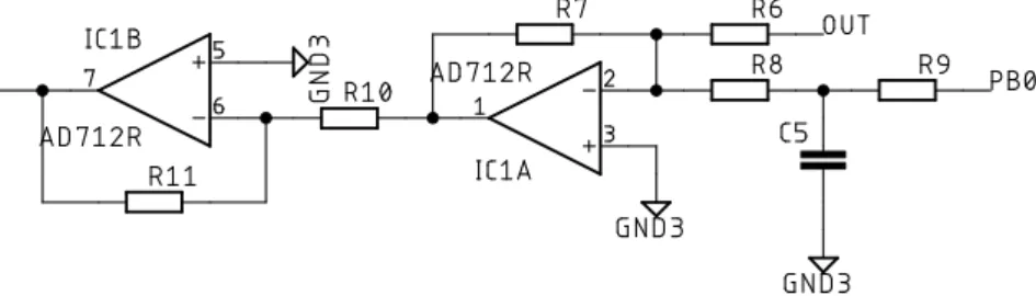
Ideally, the microcontroller is able to track the output voltage of the ADP1074 and apply the appropriate voltage at the feedback pin to set the output voltage. To this extent, the datasheet states that the ADP1074 tries to regulate itself in order to maintain a constant 1.2 V at the feedback pin. With this requirement, a circuit can be designed that makes this possible. There are a couple of possible solutions. • Use a digital potentiometer, as part of a voltage divider. The microcontroller sets the resistance of
the potentiometer, regulating the voltage on the feedback pin.
• Use a circuit that consists of operational amplifiers. This circuit would need to consist of an inverting summing amplifier (to ”mix” the actual output with the voltage set by the microcontroller). This should then be followed by a unity-gain invertor.
Not having any preference for either of the above described circuits, the second one was chosen. As such, the circuit in figure 7.3 was used. This circuit takes a inverted weighed sum of the output of the ADP1074 and a voltage set by the microcontroller. This is followed by a unity-gain invertor to make the provided voltage positive again. Limiting the output voltage of the ADP1074 to 8 V and applying the fact that
the microcontroller is limited to 3.3 V, the gain factors (and thus the resistors) can be chosen adequately.
Figure 7.3: Opamp circuit providing feedback to the ADP1074. PB0 depicts the microcontroller PWM output pin.
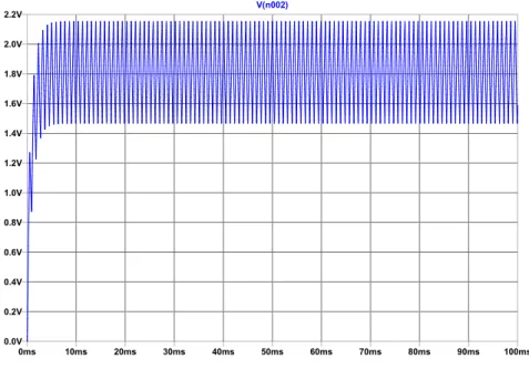
First of all, the presence of resistor R9 and capacitor C5 should be emphasised. Together, they form a lowpass filter as the microcontroller was equipped with on-chip PWM, but had no on-chip DAC (see section 7.7 for the microcontroller’s features). For the reader’s information, the PWM timer frequency is around 1100 Hz. This is based on a 72 MHz clock frequency and a 16 bit PWM timer register. Adding a lowpass filter to the PWM output comes with a couple of trade-offs. Firstly, the order of the lowpass filter is preferably kept as low as possible (increases complexity, while having very little added value). Next, there is a rise time versus voltage ripple trade-off. The larger the RC-constant, the less ripple (which is desirable), but that comes at the expense of a larger rise time (the final value is reached later, which - in some ’extreme’ situations - could lead to instability in the feedback loop). Lastly, there is the presence of the input resistor that is part of the summing amplifier. One thing to take care of is the fact that it is very undesirable if that resistor would form a voltage divider with the lowpass filter’s resistor. One could think of a couple of solutions to eliminate this, for example an active lowpass filter. Instead, the solution chosen here, was to pick a resistor that was small enough, compared to the input resistor of the summing amplifier. This comes down to a slightly larger capacitor, but certainly not very large. The characteristics of the lowpass filter are depicted in figure 7.4. In this simulation, a 50 % duty cycle was applied. This filter output shows quite a lot of ripple. This makes that later on in the project, this lowpass filter was switched for a DAC (see subsection 8.4.7).In a future design, this should be changed with either a proper on-board DAC or an active lowpass filter (thus removing the voltage dividing resistor). Other solutions could of course be thought of.
7.4
Galvanically isolated low power supply
The next part that needed to be done was to design another galvanically isolated power supply. This power supply would be used to power the microcontroller. Additionally, it would be used to create the appropriate voltages for the analog opamp circuitry. It also has a third function, it provides power to the secondary side of the ADP1074. Normally, this chip generates it’s own power for the secondary side logic from the output. In order to do this, the output voltage has to be larger than 5 V. This extra power supply is a convenient solution for this problem. The low power supply should be easier to design than the ADP1074 supply as the output voltage didn’t have the need to be dynamically variable, a fixed output voltage was desired here. To make a compromise between a 3.3 V microcontroller (with a 5V on-board low-dropout regulator) and a analog supply, able to generate maximally 19 V, a 5 V output voltage was chosen. Again, going through the different possibilities, either a flyback or a forward converter was possible. Reviewing the possible converters that were available from Analog Devices, the LT3574 flyback converter seemed a promising solution. The current requirements for the supply were not that high (only
0ms 10ms 20ms 30ms 40ms 50ms 60ms 70ms 80ms 90ms 100ms 0.0V 0.2V 0.4V 0.6V 0.8V 1.0V 1.2V 1.4V 1.6V 1.8V 2.0V 2.2V V(n002) --- C:\Users\hspildoo\Desktop\Draft4.raw ---
Figure 7.4: Lowpass filter of the feedback loop.
a microcontroller and some opamps needed power), so it would be perfect for the job. Another advantage was that also here, there was no need for an optocoupler to couple back to the primary winding. The components for this supply got ordered and were mounted on a test PCB (see figure 7.5a). The chip came in a tiny 0.65mm pitch SOIC-package. While hand soldering, on the first try, two pins of the chip got shorted out, without being able to resolve this short. The second one got on in the end, but there managed to be a short on the output, destroying that converter too. Desperate in need for a solution, a logical option would be ordering new converters, but they got out of stock (with a 14 week lead-time). Looking towards other solutions, other flyback and forward converters came to mind, but the pre-assembled kind of DC-DC converters (see figure 7.5b) also looked very promising. This converter takes a variable input voltage (in this case 9 V-36 V), and have a fixed output voltage (here 5 V), with a certain current capability (600 mA). They are isolated between input and output, come in a small form factor and easier to implement. On top of that is the price of such a converter is actually cheaper than the components of the converter. For these reasons, this solution made it in the design. This has also been used in the final design for the same reasoning.
7.5
Power supply to drive the analog circuitry
The low power 5 V supply makes sure, the solar cell can use isolated power for the logic (microcontroller, current sensor, etc). However, the solar cell makes use of a couple of operational amplifiers (for the feedback to the ADP1074 and for driving the output stage). These opamps need to be provided with power (positive and negative, with respect to the ground). This means that there is a need to have a circuit that doesn’t need to supply a lot of current, but that needs to create a positive voltage of at least +9V and a negative voltage of at least -9V. A simple solution for this problem could be found by making use of a charge pump. For these charge pump circuit, the LMC7660 of Texas Instruments was used. This integrated circuit is able to produce positive and negative voltages. To make these voltages, a two step solution was needed. The first step would need a voltage doubler. This circuit is depicted in figure 7.6a. After this voltage doubler, another LMC7660 is added. This one is being used to convert the +9V in -9V
(a) Low power isolated supply based on the LT3574 flyback converter.
(b) Low power isolated supply that comes pre-packaged.
Figure 7.5: Considered options for the low power, galvanically isolated 5 V power supply.
and create another +17V (comes free as a bonus if two diodes are added). This second circuit is given in figure 7.6b.
(a) Charge pump doubling the input voltage.
(b) Charge pump inverting the input voltage and doubling the input voltage.
Figure 7.6: Charge pump circuitry.
7.6
Output stage
Regulating the main power supply (ADP1074) is probably not a good idea. The dynamics (transfer functions) of the control loop are not mentioned, so afraid to create instability, the decision was taken to keep the output voltage of the ADP1074 constant. This also means that an analog output stage needs to designed that is able to regulate the output voltage of the solar cell emulator. Additionally, as the solar cell emulator needed to be able to function as a load too, the output stage also needed to be able to generate a negative voltage (on the positive terminal). To this extent, an analog output buffer stage in figure 7.7b is constructed. To be able to control this output stage, another operational amplifier circuit is used. The task of this opamp circuit is to steer the output, either positively or negatively, from a single PWM pin of the microcontroller. In order to do this, the circuit in figure 7.7a is proposed. This circuit first inverts the voltage of the PWM pin, then adds (and inverts) this voltage to a constant 3.3 V by means of an inverting summing amplifier. This makes for a possible positive and negative voltage, from a single 0 V to 3.3 V output. Next this voltage is unity-inverted again and applied to the buffered output stage.