RIVM report 265001001/2005
Nanotechnology in medical applications: state-of-the-art in materials and devices B. Roszek1, W.H. de Jong2 and R.E. Geertsma1
This investigation has been performed by order and for the account of the Department of Pharmaceutical Affairs and Medical Technology of the Dutch Ministry of Health, Welfare and Sports, within the framework of project V/265001, Support for Policy on Medical Technology.
RIVM, P.O. Box 1, 3720 BA Bilthoven, telephone: 31 - 30 - 274 91 11; telefax: 31 - 30 - 274 29 71 Contact:
Dr. B. Roszek, Boris.Roszek@rivm.nl
1
Centre for Biological Medicines and Medical Technology, RIVM 2
Abstract
Nanotechnology in medical applications: state-of-the-art in materials and devices
Nanotechnology is an extremely powerful emerging technology, which is expected to have a substantial impact on medical technology now and in the future. The potential impact of novel nanomedical applications on disease diagnosis, therapy, and prevention is foreseen to change health care in a fundamental way. Furthermore, therapeutic selection can increasingly be tailored to each patient’s profile. This report presents the state-of-the-art in the area of promising nanotechnology approaches for medical technology. In particular, relevant applications are reported in surgery, cancer diagnosis and therapy, biodetection of disease markers, molecular imaging, implant technology, tissue engineering, and devices for drug, protein, gene and radionuclide delivery. Many medical nanotechnology applications are still in their infancy. However, an increasing number of products is currently under clinical investigation and some products are already commercially available, such as surgical blades and suture needles, contrast-enhancing agents for magnetic resonance imaging, bone replacement materials, wound dressings, anti-microbial textiles, chips for in vitro molecular diagnostics, microcantilevers, and microneedles.
Keywords: nanotechnology; medical technology; biosensors; molecular imaging; implants; cancer diagnostics; cancer therapy; in vitro diagnostics
Rapport in het kort
Nanotechnologie in medische toepassingen: stand der wetenschap in materialen en producten
Nanotechnologie is een uitermate krachtige, opkomende technologie die op dit moment al toegepast wordt en in de toekomst een aanzienlijke invloed zal hebben op de medische technologie. Innovatieve nanomedische toepassingen kunnen de gezondheidszorg op fundamentele wijze veranderen, omdat er nieuwe mogelijkheden beschikbaar komen voor diagnose, behandeling en preventie van ziekte. Verder kunnen behandelmethodes in toenemende mate precies op maat worden gemaakt gebruikmakend van het profiel van de patiënt. Dit rapport geeft een overzicht van de “state-of-the-art” op het gebied van veelbelovende nanotechnologische ontwikkelingen in de medische technologie. Met name worden relevante toepassingen besproken in chirurgie, diagnose en behandeling van kanker, bepaling van ziekte-specifieke stoffen in het lichaam, beeldvormende technieken, implantaten, tissue engineering en toediening van geneesmiddelen, eiwitten, genen en radionucliden. Veel toepassingen van nanotechnologie in de medische technologie staan nog in de kinderschoenen. Een toenemend aantal producten wordt echter momenteel onderzocht in klinische studies en sommige zijn al commercieel verkrijgbaar, waaronder chirurgische mesjes en hechtnaalden, contrastmiddelen voor beeldvorming met magnetische resonantie, botvervangende materialen, wondbehandelingsproducten, antimicrobieel textiel, chips voor in vitro moleculaire diagnostiek, “microcantilevers” en micronaalden.
Trefwoorden: nanotechnologie; medische technologie; biosensoren; moleculaire beeldvorming; implantaten; kankerdiagnostiek; kankertherapie; in vitro diagnostiek
Summary
Nanotechnology is an emerging technology seeking to exploit distinct technological advances of controlling the structure of materials at a reduced dimensional scale approaching individual molecules and their organised aggregates or supramolecular structures. Basically, the nanometre-length scale is creating possibilities for novel materials that can be used for the construction of devices and systems. Nanotechnology must be distinguished from the nanoscience enabling such technology. Basically, nanoscience is the study of phenomena and material properties at nanoscale, while nanotechnology is applying the resulting knowledge to create novel materials and structures. Knowledge in nanoscience and nanotechnology is increasing worldwide, leading to great scientific advances. In turn, this is expected to lead to fundamental changes in the way that materials, devices, and systems are understood and created. Application in life sciences research, particularly at the cell level sets the stage for an exciting role of nanotechnology in healthcare.
In this report a general overview of the state-of-the-art in novel nanomaterials and recent advances of nanotechnology applications are presented, focussing on promising medical applications. Relevant medical areas are surgery, therapy, diagnostics, imaging, implant technology, bionics, bio-active surfaces, tissue engineering, textiles, actuators, and delivery systems. Products which are either commercially available or currently being developed at several companies are also included, illustrating the significant progress and challenges in nanotechnology.
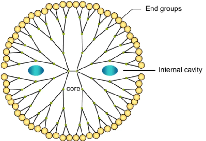
Novel nanomaterials are envisaged to have a major impact on a number of different relevant areas. Materials with high performance and unique properties can be produced that traditional synthesis/manufacturing methods could not create. Carbon nanotubes and inorganic nanowires exhibit extraordinary mechanical, electric, electronic, thermal, and optical properties offering especially the electronic industry properties that few materials platforms could ever hope to match. Although nanotube/wire electronics has been speculated about for well over a decade, the first products are now about to reach the market or are beginning to appear in the form of field emission displays, sensors, and non-volatile memory. Quantum dots (semiconductor nanocrystals) possess remarkable optical and electronic properties that can be precisely tuned by changing their size and composition. Due to their relatively inexpensive and simple synthesis quantum dots have already entered the market for experimental biomedical imaging applications. Dendrimers (complex spherical macromolecules) have improved physical, chemical, and biological properties compared to traditional polymers. Some unique properties are related to their globular shape and the presence of internal cavities offering the possibility as medical nanovehicles. In addition to these examples of individual nanoparticles, new or enhanced materials can be constructed using structural surface modifications of macro-, micro- as well as nanomaterials. Essentially, an increase in surface area and roughness attributes to an enhancement of absorbent, adsorbent, and catalytic properties. Control of surface properties at nanolevel was shown to increase the biocompatibility of the materials.
It is difficult to accurately predict the timescale of developments, but it is anticipated that within the next few years the application of nanomaterials and nanotechnology-based manufacturing will have an established role in medical technology. Some surgical aids already benefit from nano-structured material, such as surgical blades with nanometre-thick diamond coating and surface roughness in the same order of magnitude, and suture needles incorporating nano-sized stainless steel particles. Other nanotechnological approaches might allow for nanosurgery, a minimally invasive alternative to traditional surgery, based on nanoneedles and laser technologies such as optical tweezers and “nanoscissors”.
Biomedical nanotechnology presents revolutionary opportunities in the fight against many diseases. An area with near-term potential is detecting molecules associated with diseases such as cancer, diabetes mellitus, neurodegenerative diseases, as well as detecting microorganisms and viruses associated with infections, such as pathogenic bacteria, fungi, and HIV viruses. Macroscale devices constructed from exquisitely sensitive nanoscale components, such as micro-/nanocantilevers, nanotubes, and nanowires, can detect even the rarest biomolecular signals at a very early stage of the disease. Development of these devices is in the proof-of-concept phase, though entering the market may be sooner than expected. However, a different approach of molecular sensing in vivo involves the use of implantable sensors which is still hampered by unwanted biofouling impairing long-term stability of continuous sensors caused by blood components and factors of the immune system. Nanotechnology might yield nano-structured surfaces preventing this non-specific protein adsorption.
Molecular imaging is providing increasing power to studies of animal models of disease and is beginning to be used in clinical investigations as a non-invasive means of monitoring disease progress and response to therapeutics. Molecular imaging agents will allow clinicians to detect diseases in its earliest, most treatable, presymptomatic stage. Combination of precise targeting using specific antibodies and imaging enhancement properties of nanoparticles are the key to greatly enhance the power of magnetic resonance imaging, optical imaging, nuclear imaging and ultrasonic imaging. One of the great achievements foreseen is the ability to identify tumours that are far smaller than those detectable with today’s technology, before they are even visible with the human eye.
The above described advances in medical diagnostics are rivalled by the progress made in therapeutics enabled by nanotechnology. Especially in the field of cancer therapy promising applications are being developed. Several novel nanoparticles will respond to externally applied physical stimuli in ways that make them suitable therapeutics or therapeutic delivery systems. For example, magnetic iron oxide nanoparticles, gold-coated silica nanoshells, and carbon nanotubes can transform electro-magnetic energy into heat causing a temperature increase lethal to cancer cells merely by increasing the magnetic field or by irradiation with an external laser source of near-infra red light at the very location where these nanoparticles are bound to or internalised within tumour cells. Moreover, the delivery of chemotherapy and photosensitisers to tumours, and activating them in situ is possible. Also in other areas, drug delivery is one of the major application fields for nanotechnology. Nanoparticle-mediated transport across the blood-brain barrier could not only provide an effective treatment for brain tumours, but also for other central nervous system related-diseases such as Alzheimer’s and Parkinson’s. Furthermore, non-viral gene delivery systems for gene therapy, nanoneedles for cell surgery and delivery of molecules into the cell nucleus, nanocrystalline silver particles with antimicrobial activity or haemostatic agents on wound care products, microchip-based drug delivery systems for programmable drug release, and nanoporous drug eluting coatings on stents are examples of new nanotechnology materials and devices in drug delivery applications.
In the future, a modular approach to construct delivery systems which combine targeting, imaging and therapeutic functionalities into multifunctional nanoplatforms may allow for new refined non-invasive procedures. These nanoplatforms would localise to target cells, enable diagnostics and subsequently deliver therapeutics with great precision. Such modular approaches to nanodevice construction can potentially be more powerful than current treatment modalities, but are inherently more complex than existing small molecule or protein therapeutics.
Another important field of application for nanotechnology are biomaterials used for example in orthopaedic or dental implants or as scaffolds for tissue engineered products. If the design
of for example a hip implant is carried out at nanolevel, it might become possible to construct an implant which closely mimicks the mechanical properties of human bone, preventing stress-shielding and the subsequent loss of surrounding bone tissue. Furthermore, surface modifications at nanolevel of biomaterials or their coatings might greatly enhance the biocompatibility by favouring the interaction of living cells with the biomaterial, especially by their beneficial effect on cell adhesion and proliferation. Together with the control of nanoporosity allowing vascularisation and the growth of cells inside the biomaterial, the nano-structured surfaces of biomaterials also allow the creation of novel types of scaffolds for tissue-engineered products. A promising approach for the latter application are nanofibres produced using self-assembling peptides with engineering functionality and biodegradability. Medical devices for in vitro diagnostics, such as gene-, protein- or lab-on-a-chip devices, do not have any of the safety concerns associated with nanoparticles introduced into the body. Numerous devices and systems for sequencing single molecules of DNA are feasible. Nanopores are finding use as new nanoscale technology for cancer detection enabling ultrarapid and real-time DNA sequencers. In general, developments in protein-chips and lab-on-a-chip devices are more challenging compared to gene-chips and these devices are anticipated to play an important role in medicine of the future, which will be personalised and will combine diagnostics with therapeutics into a new emerging medical area called theranostics.
Nanomedicine is now within the realm of reality, though there is some concern about the safety of nanoparticles introduced in the human body. Research is in progress to address this issue. Examples of medical devices utilising nanotechnology, which are already on the market are surgical tools with enhanced properties, nano-sized contrast agents for molecular imaging, bone replacement materials constructed from nanostructured materials, pacemakers and hearing aids of reduced size and increased power, lab-on-a-chip devices for in vitro diagnostics, wound dressings containing nanocrystalline silver particles, microcantilevers, and microneedle-based systems for minimally invasive drug administration. Over the next ten to twenty years nanotechnology may fundamentally transform science, technology, and society offering a significant opportunity to enhance human health in novel ways, especially by enabling early disease detection and diagnosis, as well as precise and effective therapy tailored to the patient.
Preface
This report describes the state-of-the-art of materials and devices in the area of nanotechnology in medical applications. The review was performed on the request of the Department of Pharmaceutical Affairs and Medical Technology of the Ministry of Health, Welfare and Sports in the Netherlands. The information gathered here is presented as basic information to staff of this department who are involved in determining Dutch policy on medical technology issues, but it may also be useful for other parties in the fields of nanotechnology and/or medical technology. Concurrently, a second report was written which evaluates possible risks for human health related to the application of nanotechnology in medical practice.1
For the overview presented here, scientific literature was evaluated and included when available either in journal publication or early online publication on the internet before the 1st of August 2005.
We acknowledge the following experts for their suggestions and critical comments: Richard Moore PhD, Eucomed, Brussels, Belgium
J. Malcolm Wilkinson PhD, Technology for Industry Ltd., Ely, Cambridgeshire, UK Ineke Malsch MSc, Malsch TechnoValuation, Utrecht, the Netherlands
1 De Jong WH, Roszek B and Geertsma RE (2005). Nanotechnology in medical applications: possible risks for
Contents
1. INTRODUCTION 15
1.1 SCOPE 16
1.2 METHODOLOGY 16
2. NANOSCIENCE AND NANOTECHNOLOGY 17
2.1 DEFINITIONS 17
2.2 NANOSCALE FEATURES 17
3. NANOMATERIALS FOR THE 21ST CENTURY 21
3.1 CARBON NANOMATERIALS 21
3.1.1 Introduction: carbon bonds and structures 21
3.1.2 C60 21
3.1.3 Carbon nanotubes 23
3.1.4 Other carbon nanotube-based materials 28
3.2 INORGANIC NANOMATERIALS 29
3.2.1 Inorganic fullerene-like molecules 29
3.2.2 Inorganic nanotubes 29
3.2.3 Inorganic nanowires 30
3.2.4 Quantum dots 31
3.2.5 Dendrimers 33
3.2.6 Nanoporous material 35
4. NOVEL MEDICAL APPLICATIONS 37
4.1 SURGERY 37
4.1.1 Conventional surgical tools 37
4.1.2 Minimally invasive surgery 37
4.1.3 Optical nanosurgery 38
4.1.4 Future directions 38
4.2 NANOPARTICLES / PLATFORMS FOR CANCER THERAPY 38
4.2.1 Thermotherapy 39
4.2.2 Photodynamic therapy 41
4.2.3 Chemotherapy 44
4.2.4 Radiotherapy 45
4.2.5 Future directions in cancer therapy 46
4.3 BIOSENSORS / BIODETECTION 47
4.3.1 Cantilever array sensors 47
4.3.2 Nanotube-based sensors 49
4.3.3 Nanowire-based sensors 51
4.3.4 Other optical-based sensors 52
4.3.5 Nanoarray-based biodetection 52
4.3.6 Nanoparticle-based biodetection 52
4.3.7 Future challenges 54
4.4 IN VIVO DIAGNOSTICS USING MOLECULAR IMAGING 54
4.4.1 Magnetic resonance imaging 55
4.4.2 Quantum dots-based optical imaging 58 4.4.3 Emissive polymersomes-based optical imaging 60
4.4.4 Ultrasonic imaging 61
4.4.6 Future directions in molecular imaging 62
4.5 IMPLANTABLE MATERIALS FOR ORTHOPAEDICS AND DENTISTRY 63
4.5.1 Implant coatings 63
4.5.2 Surface modifications 66
4.5.3 Bone replacement materials 67
4.5.4 Tissue Engineering 67
4.6 IMPLANTABLE MATERIALS FOR VASCULAR INTERVENTIONS 68
4.6.1 Stent coatings 69
4.6.2 Stent coatings with drug-eluting capacity 69
4.7 ACTIVE IMPLANTABLE DEVICES AND BIONICS 69
4.7.1 Vision rehabilitation 70
4.7.2 Pacemakers and hearing aids 71
4.7.3 Neuro-engineered systems for motor control 72 4.7.4 Microchip-based drug delivery systems 72
4.7.5 Prosthetic knee system 73
4.7.6 Current and future developments 73
4.8 TEXTILES AND WOUND CARE PRODUCTS 74
4.8.1 Antimicrobial textile surfaces 74
4.8.2 Biomedical “smart” textiles 75
4.8.3 Wound care products 76
4.9 CHIPS FOR MOLECULAR DIAGNOSTICS 76
4.9.1 DNA microarrays 77
4.9.2 Protein microarrays 78
4.9.3 Lab-on-a-chip 79
4.9.4 Cell chips 80
4.9.5 Future directions in novel chip systems and molecular diagnostics 81
4.10 DELIVERY DEVICES / TOOLS 82
4.10.1 Needles for administration and monitoring 82 4.10.2 Nanomaterials for brachytherapy and nanocapsules 84 4.10.3 Nanoparticles for drug delivery across blood-brain barrier 84 4.10.4 Nanotube-based delivery applications 85
4.10.5 Nanovectors for gene therapy 86
5. CONCLUSIONS 87 REFERENCES 89
APPENDIX A – HISTORICAL PERSPECTIVE 115
APPENDIX B – CARBON NANOTUBES 117
APPENDIX C – BIOSENSORS 123
1.
Introduction
Technology is generally regarded as the utilization or application of science to benefit society. Nanotechnology is an emerging technology, which is no longer just a vision for the future as it was generally seen at the end of 20th century. Instead, nanotechnology is a ubiquitous technology with a potential to impact on every aspect of modern human civilization. An incredibly diverse range of areas will be affected, such as agriculture, communication, energy generation/transmission, computers, environmental monitoring, food manufacturing/processing, health care, personal care, space travel, robotics, but probably the biggest impact will be in medical technology.
In general, nanotechnology is acknowledged to represent a new frontier in science and technology of the 21st century. One may argue, however, that nanotechnology is not as contemporary as it seems to be. Although the word nanotechnology is relatively new, the “natural version” of nanotechnology was already in pole position with procreation of life itself thousands of millions of years ago (see Appendix A). All natural materials and systems establish their foundation at the nanoscale. Basically, the biological building blocks of life are nano-entities that possess unique properties determined by the size, folding, and patterns at nanoscale. The genetic material desoxyribonucleic acid (DNA) is composed of four nucleotide bases in sizes ranging in the sub-nanometre scale, and the diameter of the double-helix structure of DNA is in the nanometre range. The same is true for proteins and cell membranes which consist of lipids and proteins.
Manufacturing “non-natural” nanomaterials faces many challenges, often requiring a specific approach. Miniaturisation has been applied quite successfully for some decades now. This “top-down” approach has traditionally been used in the fabrication of electronics in the semiconductor technology industry. However, nanotechnology is more than miniaturisation alone. In order to explore the full potential of nanotechnology a new paradigm has to be set. This is accomplished by a “bottom-up” approach building structures from more basic materials. Self-assembly is a bottom-up technique that attracts much attention. In fact, this concept is not new. Biological systems are built predominantly using self-assembly. What is new is the enhanced ability to “externally” or “specifically” or “intentionally” control the structure at the nanoscale and manufacture new materials such as nanotubes, nanowires, and nanocapsules.
Nanomaterials are difficult to maintain as individual particles. One reason for this is their marked propensity to agglomerate because agglomeration reduces the enormous surface area in relation to the volume of the nanomaterial, which is energetically unfavourable. Appropriate “bottom-up” approaches and applying precision surface engineering may overcome agglomeration.
Nevertheless, nanotechnology offers very interesting possibilities of developing new innovative products for many areas of daily life, some of which have already been realised. Also the field of medical technology has already started to benefit from the progress in nanotechnology. Many revolutionary applications, such as novel sensing technologies, surface modifications, and implant technologies are currently being developed. Probably the most significant impacts of nanotechnology will be at the biomaterials/living tissue interface and the non-biological/cell interface, e.g. human-machine (for example retinal prosthesis). Whether a prosthetic implant is accepted or rejected, whether a drug is effective or whether living tissue will regenerate are all questions which could be approached at the nanometre scale. Interfacing materials with human biology/physiology is one of the exciting new
frontiers of nanotechnology in the field of medical applications. Nanotechnology will definitely be a strategic branch for science and engineering during the coming century. It will fundamentally restructure the technologies currently used for manufacturing, medicine, communication, computation, transportation and many other application areas.
1.1
Scope
This report focuses on recent advances of nanotechnology applications in medical technology. An overview of the state-of-the-art in nanomaterials and (medical) devices is given. Relevant medical areas are surgery, therapy, diagnostics, imaging, implant technology, bio-active surfaces, tissue engineering, textiles, actuators, and drug/gene delivery materials and systems. Products that are already on the market or are currently being developed illustrate the significant progress in nanotechnology.
1.2
Methodology
The state-of-the-art in nanomaterials and devices was based on literature searches, internet searches, and proceedings of conferences. Literature was identified from several sources including electronic databases and cross-checking of reference lists. Electronic databases consulted were Scopus™ (Elsevier BV) and PubMed (US National Library of Medicine). Searches were restricted to a selection of the most relevant application areas of medical technology due to the vast number of publications. Several conferences on medical applications of nanotechnology were attended and some topics discussed were included in this report. Product information was obtained using manufacturers’ websites retrieved from Google (www.google.com) or Nanovip.Com, a web-searchable database focused on nanotechnology companies. It should be noted that applications of nanotechnology in drug discovery research, providing tools for a fast screening of large arrays of candidate substances, were not included in the report. Furthermore, applications on liposome-based drug delivery and viruses as delivery vehicle were excluded.
In order to be able to place the nanotechnology applications in medical technology in the right perspective, it is necessary to have a basic understanding of the origin of the unique properties of nanomaterials. Therefore this report starts with a short section explaining the definitions and features of nanoscience and nanotechnology, followed by a more elaborate overview of the novel nanomaterials and their specific properties which have opened the horizon for the applications in medical technology which are described in the main part of the report. Furthermore, in this report greater emphasis is given on highlighting promising nanotechnology-based approaches in medical technology than on consensus taxonomies of scientific/engineering disciplines.
2.
Nanoscience and nanotechnology
2.1
Definitions
In a recently published report of The Royal Society & The Royal Academy of Engineering (2004) definitions were given for nanoscience and nanotechnology:
Nanoscience is the study of phenomena and manipulation of materials at atomic,
molecular and macromolecular scales, where properties differ significantly from those at larger scale.
Nanotechnology is the design, characterisation, production and applications of
structures, devices and systems by controlling shape and size at the nanometre scale.
2.2
Nanoscale features
The prefix nano is from the Greek word nanos (νανοσ) which means dwarf. Commonly, nano is associated with the SI length unit metre and denotes one-billionth (10-9). Thus, nanomaterials are characterised at the nanometre scale in one, two or three dimensions, leading to quantum wells (e.g., thin films, layers, surface coatings), quantum wires (e.g., nanotubes, nanowires) or quantum dots (qdots), respectively (Figure 1). Nanoparticles with a diameter of less <100 nm are for example fullerenes, dendrimers and semiconductor quantum dots.
Figure 1. Progressive diminishing of size up nanometre dimensions for rectangular structures. The principle is also valid for curvilinear structures, such as spheres, discs and tubes.
The word quantum is associated with these three structures because profound changes in material properties emanate from the quantum mechanical nature of physics that rules the world in the ultra-small and where material properties no longer obey the classical macroscopic laws of physics. Materials can be scaled down many orders of magnitude from macroscopic to microscopic without any or little change in expected properties occurring. However, when the nanoworld is entered, characteristic changes are observed. For the time
being no strict dimensional limits can be defined for this phenomenon. At the nanoscale, physics, chemistry, biology, material science, and engineering converge toward the same principles and tools. As a result, progress in nanoscience will have very far-reaching impact. The nanoscale is not just another step toward miniaturisation, but a qualitatively new scale. The change in behaviour is dominated in the first place by quantum mechanics, as mentioned above and is additionally attributable to material confinement in small structures, and the increase in surface area per volume (or mass unit) (Figure 2). At the larger end of the nanometre scale other phenomena are crucial, such as surface tension and Brownian motion.
Figure 2. Interrelationships of radius, surface area, and volume of a quantum dot. Note that the volume decreases more rapidly than surface area for a given decrease in radius. Hence, surface area to volume ratio increases dramatically for a lower radius compared to the ratio for a higher radius. Drawn to scale approximately.
Nanoscience is concerned with understanding these effects and their influence on material properties. Nanotechnology aims to exploit these effects to create structures, devices, and systems with novel properties and functions due to their size (The Royal Society & The Royal Academy of Engineering, 2004). In contrast to other key technologies, such as
r = 2 nm r = 6 nm Radius r = 8 nm Surface area A = 806 nm2 A = 454 nm2 A = 50 nm2 V = 34 nm3 V = 905 nm3 Volume V = 2145 nm3
biotechnology, information and communication technology, nanotechnology is much less well-defined and well-structured. In fact, nanotechnology is immensely complex and covers multiple disciplines ranging from physics, chemistry, and biology to engineering disciplines. This is reflected by the enormous number of publications which accelerated from 1989 onwards (Compañó and Hullmann, 2002). In 1989 about 1000 scientific articles have been published. In 1998 the number increased to more than 12.000 publications. Data for 1999 and 2000 confirm the continuation of this development (Hullmann and Meyer, 2004). Concurrently, patents as indicators of output of applied research showed a progressive increase.
3.
Nanomaterials for the 21
stcentury
This chapter is concerned with various new or enhanced nanomaterials that are envisaged to have a major impact on technological applications in general and medical technology in particular. Nanomaterials are categorized into carbon and inorganic nanomaterials. It should be noted that not only nanoparticles are discussed, but also nano-structured bulk materials, because the physical interactions at the nano-scale interface between biological structures and materials are crucial for the biological response.
3.1
Carbon nanomaterials
3.1.1 Introduction: carbon bonds and structures
The bonds between carbon atoms are such as to follow the formation of some of the most interesting nanostructures. Solid carbon at room temperature has two classical structures or allotropes: diamond and graphite. In diamond, carbon atoms are connected each to four other carbon atoms in a tetrahedral lattice structure and these bonds form a three-dimensional network. Diamond is the hardest mineral known to man and is an excellent electrical insulator. In graphite the carbon atoms are arranged in hexagons and strongly bonded into parallel planar sheets. The sheets are held together by much weaker Van der Waals forces, which is the reason why graphite can be used as material in pencils and as the basis of some lubricants. Unlike diamond, graphite is a conductor of electricity. As illustrated by these classical examples, physical properties can vary considerably within pure carbon materials. 3.1.2 C60
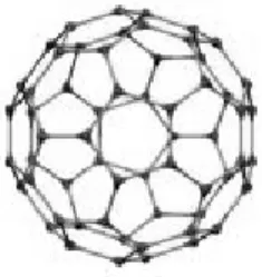
In 1985 the discovery of the existence of a third and new carbon allotrope containing sixty perfectly symmetrically arranged carbon atoms (C60) meant a major breakthrough and opened a novel field of carbon chemistry (Kroto et al., 1985). The C60 molecule was originally and formally called buckminsterfullerene after the American architect and inventor R. Buckminster Fuller (1895-1983), who designed geodesic domes similar to the structure of C60. Scientists quickly nicknamed it a “buckyball” as the spherical structure of C60 resembles a football (Figure 3).
Figure 3. Representation of a C60 molecule. Source: ©Chris Ewels 2003 (www.ewels.info).
The geometric configuration consists of 60 vertices and 32 faces, 12 of which are pentagonal and 20 hexagonal. The faces are symmetrically arrayed to form a molecular ball with a
diameter of approximately 1.0 nm. Soon after the discovery of C60 many other fullerene molecules with variable shapes and forms have been synthesized, such as C70, C76, C80, and C84 (Dresselhaus et al., 1996). The higher fullerenes are also interesting and hold several promises in their own right.
Synthesis
Initially C60 was produced by vaporisation of graphite into helium using a laser beam (Kroto et al., 1985). This process was not scalable and could not produce the larger quantities necessary for commercial availability. Therefore, only few experiments could be performed on the material and comprehensive fundamental research or even evaluating possible applications was restricted. However, in 1990 C60 molecules and other fullerenes could be produced in bulk quantities, i.e. macroscopic gram amounts, using an electric carbon arc discharge apparatus (Krätschmer et al., 1990). Evaporating graphite electrodes in helium under low pressure (0.1 atm) yielded 100 mg of pure material in one day, approximately. This opened completely new possibilities for experimental research and industrial use. In 1991, a new method of fullerene production was invented, providing basic engineering knowledge critical to scale up the process (Howard et al., 1991). This synthesis method involves the combustion of hydrocarbon fuel under sub-atmospheric pressure and makes economical production of higher fullerenes possible. Refining and improving the production process is still continuing. C60 remains the easiest to produce and cheapest ($100/gram, C purity >99.9%) with prices increasing progressively for the larger fullerenes ($500/gram for C78, C purity >98%) (Bucky USA, Houston, Texas, 2004). Several companies hope to produce tens of metric tons a year in the near future, which could reduce the price down to $0.20/gram.
Properties and applications
C60 has appealing physical, (bio)chemical, electrical and optical properties. These properties can be modified by functionalization, i.e. attaching chemical groups to a fullerene’s carbon atom. When crystalline C60, normally an insulator, is doped with alkali metals, such as potassium, caesium or rubidium, it can be made metallic (Haddon et al., 1991). Various functionalizations have been utilised to increase hydrophilicity of fullerenes as well as to prepare new compounds with biological and pharmacological activity (Bosi et al., 2003). C60 derivatives have a high physical and chemical affinity for the active site of various enzymes, such as HIV-1 protease (Friedman et al., 1993; Schinazi et al., 1993; Sijbesma et al., 1993). Introducing a C60 molecule into the catalytic cavity of HIV-1 protease inhibits this fundamental enzyme for virus survival. Evidence has been found for superconductivity (Hebard et al., 1991) and currently C60 is being investigated in artificial photosynthetic applications, e.g. photovoltaic devices (Cho et al., 2005). Fullerenes are powerful antioxidants, reacting readily and at a high rate with free radicals, which are often the cause of cell damage or death (Chueh et al., 1999; Lin et al., 1999; Straface et al., 1999). Fullerenes could hold promise in health and personal care where prevention of oxidative cell damage or death is desirable.
The entrapment of (metal) atoms inside the cavity of C60 or other fullerenes is known as a nanomaterial family called endohedral (metallo)fullerenes. Endohedral fullerenes are described with the notation X@C60, where X is the caged atom (or atoms) and C60 could be any fullerene. Reactive elements can be stabilised inside the fullerene cage. Moreover, entrapped elements can change the electrical and magnetic properties of the fullerene molecule. Because endohedral fullerenes are resistant to metabolism and highly kinetically stable, they can be used as carriers for biomedical in vivo imaging (Cagle et al., 1999) (see Section 4.4.1).
3.1.3 Carbon nanotubes
Carbon nanotubes are among the astonishing objects that science sometimes discovers and which will likely revolutionize technological developments of the 21st century. As the fourth allotrope of carbon, carbon nanotubes are also molecules consisting solely of carbon atoms. They can be considered as elongated fullerenes. Though the expectations of fullerenes were quite high after their discovery, only few applications have actually reached the market. However, for carbon nanotubes enthusiastic predictions are being made as their physical properties, i.e. mechanical, electronic, thermal and optical, exceed those of commonly used materials.
In 1991 Sumio Iijima reported the existence of concentric multi-walled carbon nanotubes (MWCNTs) as by-products of the formation of fullerenes (Iijima, 1991). The real breakthrough occurred two years later when two research groups (Bethune et al., 1993; Iijima and Ichihashi, 1993) independently discovered, again unexpectedly, single-walled carbon nanotubes (SWCNTs) consisting of a single seamless cylindrical wall of carbon atoms. MWCNTs can be considered as a collection of concentric SWCNTs with different diameters similar to cylinders within cylinders. SWCNTs were really new nano-objects having specific properties and behaviours. Recently, double-walled carbon nanotubes (DWCNTs) have been synthesized in pure form (Endo et al., 2005b). These intermediate structures are likely to have superior material properties and could replace MWCNTs or SWCNTs in several applications.
Structure
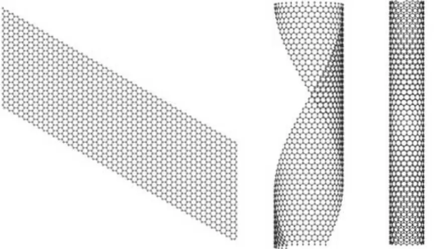
Carbon nanotubes are in essence rolled-up, highly ordered hexagonal carbon honeycomb sheets, which at the end can be closed or open (Figure 4). A detailed description of the topology of carbon nanotubes is included in Appendix B.1.
Figure 4. Illustration of a flat carbon sheet (left) up into a partially rolled-up sheet (middle) and carbon nanotube (right). Source: ©Chris Ewels 2003 (www.ewels.info).
At least one dimension of the tube should be 100 nm or less. Calculations have shown that a diameter greater than 2.5 nm is energetically not favourable to maintain a tubular morphology (Tersoff and Ruoff, 1994). Although SWCNTs with diameters of 0.4 nm have been synthesized (Wang et al., 2000), a suitable energetic compromise is reached for ~1.4 nm, the most frequent diameter encountered in SWCNTs regardless of the synthesis techniques. The
smallest, stable, SWCNT grown inside a MWCNT is just 0.3 nm in diameter and has only four hexagons around its circumference (Zhao et al., 2004a). The length of carbon tubes is not as restricted, depending on the synthesis conditions and varies from tens of micrometers to hundreds, or more. Recently, a research team in the USA has established a record length synthesizing four centimetres long individual SWCNTs (Zheng et al., 2004b). Moreover, long strands of ordered SWCNTs with a length of ~20-30 cm, a strand diameter of 0.3-0.5 mm and carbon nanotube diameter of ~1 nm have also been accomplished (Quy et al.,
2005; Zhu et al., 2002). Nowadays SWCNTs can be grown continuously without any apparent length limitation (Wang et al., 2005b). These physical dimensions make SWCNTs unique examples of molecules with enormous aspect ratios (ratio of length to diameter) and can be considered as nearly one-dimensional structures.
Synthesis
Several technologies (solid and gaseous carbon-based production techniques) are currently used to make carbon nanotubes, including electric arc discharge (Ebbesen and Ajayan, 1992; Iijima, 1991), laser ablation (Guo et al., 1995; Thess et al., 1996), and chemical vapour deposition (Kong et al., 1998; Li et al., 1996; Ren et al., 1998) (see Appendix B.2). The exact growth mechanism of carbon nanotubes is not fully understood yet.
The synthesis processes vary considerably with respect to structural quality, purity, scalability, and type of carbon nanotube synthesized, i.e. morphology and helicity. In general the synthesis yields a mix of different kinds of carbon nanotubes, some metallic and some semiconducting. The purification of SWCNTs is difficult to perform since SWCNTs can have defects and contain a lot of metal catalyst. Scalability of production processes is an essential commercial prerequisite. Some methods use equipment that simply cannot be made bigger and the only way to increase production is to make more pieces of equipment, which will not decrease costs significantly. On the long term laser-based methods are generally considered not competitive compared to the chemical vapour deposition method providing good perspectives of large-scale and low-cost processes for the mass production of carbon nanotubes.
SWCNTs were first marketed by Carbon Nanotechnologies, Inc. (Houston, Texas, USA) with prices as high as $1000/gram for raw material in 2002. Prices are steadily declining with Nanoledge S.A. (Montpellier, France) offering SWCNTs, though synthesized by the electric arc method, at a price of €65/gram (2005 data). For the time being SWCNTs synthesized using the chemical vapour deposition method yield a slightly higher price of ~$200-400/gram which is marketed for example by Nanostructured & Amorphous Materials, Inc. (Los Alamos, New Mexico, USA). Getting to the market has been hampered by high prices and production bottlenecks. However, some forty global producers have now reached a point where the combination of decreasing prices and increased availability will enable more widespread applications. In the near future prices as low as $0.03/gram of raw high concentration SWCNTs soot are expected. Other major European suppliers of carbon nanotubes are Thomas Swan & Co., Ltd. (Consett, Durham, UK) and Nanocyl S.A. (Sambreville, Belgium).
Mechanical properties and applications
Several studies have been performed to characterize the extraordinary mechanical properties of carbon nanotubes. For a recent review on this topic see Dresselhaus et al. (2004). Young’s modulus (a measure of the stiffness of a material) of carbon nanotubes is larger than that of any known material (see Box 1). Carbon nanotubes have also remarkable tensile strength that is a multiple tenfold of steel (Yu et al., 2000c). Defect-free MWCNTs with tube ends well capped are expected to have very high tensile strength. Although it is difficult to perform
such measurements in a reliable manner, a tensile strength value of ~150 GPa has actually been measured for electric arc MWCNTs (see Appendix B.3).
Carbon nanotubes are exceedingly tough materials. MWCNT can be bent repeatedly without undergoing catastrophic failure, suggesting that they are remarkably flexible and resilient (Falvo et al., 1997). The extraordinary flexibility and resistance to fracture distinguishes carbon nanotubes from graphitic fibres as engineering material. The ability of carbon nanotubes to elastically sustain loads at large deflection angles enables them to store or absorb considerable energy (Wong et al., 1997).
Box 1. Mechanical properties of materials compared to carbon nanotubes
Specimen Young’s modulus Reference
Human chondrocytes 0.7 kPa (Jones et al., 1999) Human cartilage 0.7 MPa (Mow et al., 1980)
Human tendon 550-1200 MPa (Maganaris and Paul, 1999) Human subchondral bone (wet, micro) 1.2 GPa (Choi et al., 1990)
Human cancellous bone (dry/wet, micro) 1-20 GPa (Rho et al., 1993) Human cortical bone (wet, micro) 5.4 GPa (Choi et al., 1990) Human cortical bone (wet, macro) 14-20 GPa (Reilly et al., 1974) Human cortical bone (dry, submicro) 23 GPa (Rho et al., 1997) Titanium alloys (commercial) 110 GPa (Lynch, 1989) Plain carbon steel 205 GPa (Lynch, 1989)
Diamond 1.04 TPa (Dresselhaus et al., 1996)
Graphite 1.06 TPa (Dresselhaus et al., 1996)
MWCNT 0.81 TPa (Salvetat et al., 1999)
0.91 TPa (Demczyk et al., 2002) 1.28 TPa (Wong et al., 1997) 1.81 TPa (Treacy et al., 1996)
SWCNT 1.00 TPa (Yu et al., 2000a)
1.25 TPa (Krishnan et al., 1998) TPa = 1000 GPa
Carbon nanotubes are potentially the ultimate material for high-strength materials applications such as reinforcement of composite materials or cable components. Applications in sports engineering are emerging, such as VS Nanotube Power and VS Nanotube Drivemade tennis rackets ($200.-) made of high modulus graphite and carbon nanotubes by Babolat VS North America, Inc. (Boulder, Colorado, USA) and Synergy SL hockey sticks and bicycle components (e.g. handlebars) incorporating Zyvex’s NanoSolve™ carbon nanotechnology by Easton Sports, Inc. (Van Nuys, California, USA). Mechanical applications could also be in armour, although a suitable matrix must be chosen to exploit the mechanical properties in a macroscopic product. Furthermore, the exceptional mechanical properties make carbon nanotubes ideal tips for force sensors in scanning probe microscopy, such as atomic force microscopy (Dai et al., 1996; Hafner et al., 2001). The carbon nanotube ends can also be specifically functionalised or coated with metals allowing improvement of imaging techniques in chemical force microscopy or magnetic force microscopy, respectively (Cheung et al., 2000; Deng et al., 2004; Wong et al., 1998). MWCNT scanning probe tips can be bought from Seiko Instruments, Inc. (Chiba, Japan), Daiken Chemical Co., Ltd. (Osaka, Japan) and Piezomax, Inc. (Middleton, Wisconsin, USA). Theoretically, these extraordinary mechanical properties would provide unique opportunities to engineer carbon nanotube-reinforced composites for orthopaedic and dental implants when embedded into appropriate matrices (e.g., metals, ceramics, and polymers) (see Section 4.5).
Electric and electronic properties and applications
Carbon nanotubes have exceptional electric and electronic properties. They are metallic or semiconducting depending on the precise structure, i.e. the helicity and diameter of the tube (see Appendix B.4) (Hamada et al., 1992; Mintmire et al., 1992; Saito et al., 1992). Metallic carbon nanotubes can transport very high current densities of up to 109 A/cm2 without being damaged (Yao et al., 2000). Normal metal wires (e.g. copper, gold) can transport current up to 105-106 A/cm2 and higher currents would vaporise these metals because of resistive heating. Metallic carbon nanotubes conduct electricity with essentially no resistance at room temperature. This phenomenon is known as ballistic transport, where the electrons can be considered as moving freely through the structure, without any scattering from atoms or defects (Javey et al., 2003; White and Todorov, 1998). In the following section highlights of some current or potential applications, made possible because of the electric and electronic properties, are described. A more elaborate description of the possibilities with the appropriate references can be found in Appendix B.4.
Field emission applications
Carbon nanotubes can be used for flat panel displays, lighting applications such as vacuum-tube elements, household light bulbs and flat panel luminescent lamps, gas discharge vacuum-tubes, X-ray generators, and electron guns for the next generation scanning electron microscopes and transmission electron microscopes. In 1999 the world’s first 4.5-inch flat panel device using carbon nanotubes was developed by Samsung Advanced Institute of Technology. Carbon nanotubes might be an alternative to bulky cathode-ray tubes, such as used for televisions and computer monitors, and the more recent liquid-crystal panels and plasma displays. Based on prototypes, the advantages of carbon nanotubes in flat panel displays are suggested to be low power consumption, high brightness, viewable from any angle, fast response rate, wide operating temperature range, no burn-in, lightness, and thinness. Other major companies involved are Motorola Labs and Eikos. Nanotube-based cold cathodes for compact, portable, and miniature ray generators are manufactured by Xintek, Inc. These X-ray tubes can be set up in a narrow space and possibly X-X-ray endoscopic imaging and provide improved high-resolution images in industrial, biological and medical applications.
Nanoelectronic applications
As carbon nanotubes behave like electrical conductors or semiconductors, they could be extremely useful for nanoscale electronics applications. An all-carbon-based nanoelectronic technology can be foreseen in which the electric wiring consists of metallic carbon nanotubes and the active devices are made of semiconductor carbon nanotubes. A lot of progress is yet to be achieved before routine production of carbon nanotube-based integrated circuits becomes possible, though it is currently feasible in an experimental set-up to build a nanocircuit that has wires, switches and memory elements made entirely from carbon nanotubes and other molecules. Currently, Nantero Inc. (Woburn, Massachusetts, USA) is developing NRAM™, a high density non-volatile random acess memory chip using carbon nanotubes as the active memory elements.
Chemical gas sensors
Semiconductor SWCNTs are highly sensitive to detect changes in the chemical composition of the surrounding atmosphere at room temperature. Carbon nanotube-based chemical gas sensors have great (commercial) potential in numerous areas ranging from medical applications, environmental monitoring, agricultural applications to the chemical industry and beyond. Currently, Nanomix Inc. is developing a medical capnography sensor (see Section 4.3.2).
Shielding material for electromagnetic radiation
A plastic composite of carbon nanotubes could provide shielding for electromagnetic interference which is of much concern to military applications. Nowadays command, control and communications are highly digitised and the system must be protected from weapons that emit electromagnetic pulses.
Battery technology
Carbon nanotubes can be used as additives in lithium-ion battery systems, lead-acid batteries, and electric double-layer capacitors improving their performance. The merit of electric double-layer capacitors is their high discharge rate, which make them applicable as hybrid energy source for electric vehicles and portable electric devices. Implantable active medical devices relying on battery technology for device powering could benefit from extended battery lifetime reducing the need for early replacement.
Electromechanical actuators
Carbon nanotubes are not only capable of sensing but also of actuation. Application of an external stimulus, such as an electrical charge, can change the dimensions of the materials reversibly. Termed “artificial muscles”, such actuators provide wonderful opportunities. An “artificial muscle” has been made consisting of two SWCNT-based paper strips on both sides of an insulating double-layer side tape suspended in a liquid environment. Another example is nanotweezers able to grab, manipulate, and release nano-objects. Carbon nanotube actuators could potentially be used in hostile environments such as in robotics used for planetary exploration, and in medical applications.
Thermal properties and applications
Prior to the discovery of carbon nanotubes, diamond was the best thermal conductor with the highest thermal conductivity of 2600 W/m·K for blue diamond at room temperature. Deduction of experimental values and theoretical calculations for SWCNTs yielded a thermal conductivity ranging from 2980 up to 6600 W/m·K (Berber et al., 2000; Che et al., 2000; Hone et al., 1999; Hone et al., 2001).
These thermal properties are of great importance for thermal management of nano/microelectronic devices. As over the past decades engineers have scaled down silicon-based devices to create very dense arrays of devices for information processing, rapid overheating poses serious problems. Dissipation of heat is widely accepted as a prerequisite for the next step in miniaturisation of electronic devices. Theoretically, carbon nanotubes could efficiently transport heat away from the chip and cool smaller chip circuits.
Fluorescence properties and applications
Fluorescence of carbon nanotubes can be added to the list of unique physical properties. A groundbreaking discovery in 2002 showed that dozens of varieties of semiconductor SWCNTs emitted their own unique fluorescent signature (Bachilo et al., 2002; O'Connell et al., 2002). Fluorescence occurs when a substance (or molecular probe) absorbs high-energy photons of a defined light source and emits a signal with different spectral characteristics (lower-energy photons) in response. The spectral characteristics can be resolved with an emission filter and captured by a high-sensitivity camera. Generally, laser sources are used because they offer power delivery at narrower and better-defined spectral windows. SWCNTs absorb and emit light in the near-infrared spectrum (700-1000 nm) where human tissue and biological fluids are particularly transparent (Wray et al., 1988). In biological tissue, for instance leukocytes, SWCNTs retain their optical properties, and cell properties such as shape, rate of growth, and ability to adhere to surfaces, are not affected (Cherukuri et al.,
2004). Unlike most single molecules (Trautman et al., 1994) or semiconductor nanoparticles (Nirmal et al., 1996), the fluorescence of SWCNTs does not show any spectral or intensity fluctuations which could enable a stable infrared photon source.
Potential medical applications are envisaged in cancer therapy (see Section 4.2.1) and in fluorescence-based biosensors (see Section 4.3.2). Although long-term studies on toxicity and biodistribution must be completed before carbon nanotubes can be applied in medical tests, the fluorescence properties indicate that carbon nanotubes could be useful as imaging markers in laboratory in vitro studies, particularly in cases where the bleaching, toxicity and degradation of more traditional markers are problematic. Moreover, since carbon nanotubes fluoresce with a single wavelength of light, it may be possible to tailor different sizes of nanotubes and tune their electrical properties to seek specific targets, and thus diagnose multiple diseases in a single test. In addition to biomedical applications, fluorescence properties of carbon nanotubes could be useful in compact, easy-to-integrate nanophotonic devices.
3.1.4 Other carbon nanotube-based materials
Doped carbon nanotubes
Carbon atoms in all types of nanotubes can be substituted with another element such as boron and/or nitrogen. Synthesis of these B- and/or N-doped carbon nanotubes was first reported in 1994 (Stephan et al., 1994). Besides partial substitution, carbon can be completely exchanged. An amazing result of such attempts is a sandwich-like structure made of multi-layered concentric nanotubes whose constituting coaxial tubes are alternatively made of carbon graphenes and boron nitride graphenes (Suenaga et al., 1997). Synthesis techniques are similar to those used for the synthesis of pure carbon nanotubes, i.e. arc discharge, laser ablation, and chemical vapour deposition. For an overview see e.g., Ma et al. (2004). The benefits of doping are better control of electronic properties of nanotubes and for low concentrations of dopants (<0.5 %) mechanical properties do not deteriorate. For instance, B-doped MWCNTs exclusively exhibit metallic conductivity (Carroll et al., 1998) in contrast to pure carbon nanotubes whose properties vary between metallic and semiconducting depending on helicity and diameter. Other benefits are enhanced field emission of B-doped (Charlier et al., 2002) and N-doped MWCNTs (Golberg et al., 2003) compared to undoped MWCNTs, i.e. turn-on voltages of ~1, 2, and 3 V/µm, respectively. Thus, both B- and N-doped carbon nanotubes may have great potential as building blocks for stable and intense field emission sources. Moreover, N-doped MWCNTs can be used as gas sensors exhibiting fast response (<1 s) and saturation within 2-3 s (Villalpando-Paéz et al., 2004). N-doped MWCNTs are good candidates for the detection of low vapour concentrations of acetone, chloroform, and ethanol, important in the fabrication of alcoholmeters. Li-ion rechargeable batteries could also benefit from the N-doped MWCNTs (Mukhopadhyay et al., 2002).
Endohedral carbon nanotubes
The inner cavity of SWCNTs or MWCNTs can be filled, partially or entirely, by other atoms, molecules, compounds, or crystals. Similar to the case of fullerenes such hybrid nanotubes are denoted as X@SWCNT or X@MWCNT where X is the atom, molecule, etc. involved. For the first time in 1998 SWCNTs were filled with C60 by thermally annealing C60 powders over SWCNTs at >600 °C under vacuum (Smith et al., 1998). C60 molecules are arranged as a self-assembled chain within the SWCNT resembling a nanoscopic peapod. Endohedral fullerenes have also been introduced inside SWCNTs and more complex nanotube-based hybrid materials have been synthesized such as Gd@C82@SWCNTs (Suenaga et al., 2000). Nanotube-based hybrid materials could be applied in electronics and micro-electro-mechanical systems. In general, though, fullerenes, carbon nanotubes and peapods have yet to
find extensive (bio)medical applications, in part because of their extreme hydrophobicity, presumably poor biocompatibility, and high chemical stability. But controlled functionalization of these carbon nanomaterials may be used to modify these features (Sayes et al., 2004).
Functionalised carbon nanotubes
Functionalisation of carbon nanotubes has important consequences for their properties and applications. Although covalent attachment of molecules on the nanotube sidewalls proves to be difficult, functionalisation by non-covalent adsorption of (biological) molecules is easier. Non-covalently functionalised SWCNTs preserve the sp2 hybrid bonds (no bonds are broken)
and thus the carbon nanotube electronic structure, and provide sites for selective binding (Chen et al., 2001). The unique properties of carbon nanotubes when utilised in conjunction with biomolecular recognition capabilities (e.g., antibodies) could lead to miniature electronic devices, including probes and sensors. Properties and applications of functionalised carbon nanotubes have been reviewed recently (Sun et al., 2002).
3.2
Inorganic nanomaterials
3.2.1 Inorganic fullerene-like molecules
Theoretical studies suggest that fully inorganic fullerene-like molecules comprising C60 analogs with silicon atoms and group 13/15 (e.g. boron-nitrogen) should be realisable, but experimental confirmation has been lacking. Recently, the synthesis and structural characterisation of soluble and entirely inorganic spherical fullerene-like molecules have been reported incorporating Cu, Cl, Fe, C, P, and N (Bai et al., 2004). These molecules are currently only of scientific interest and no applications are yet foreseen.
3.2.2 Inorganic nanotubes
Synthesis
The synthesis of various inorganic nanotubes has been reported during the last few years (for a recent review see Tenne and Rao (2004)). The structure of inorganic nanotubes is comparable with the structure of carbon nanotubes. Some of the important inorganic nanotubes synthesized are chalcogenides, e.g. MoS2 (Chhowalla and Amaratunga, 2000), oxides, e.g. TiO2 (Kasuga et al., 1998), nitrides, e.g. BN (Gleize et al., 1994), halides, e.g. NiCl2 (Hacohen et al., 1998), and metals, e.g. Ni (Bao et al., 2001). Synthesis techniques are similar to those of carbon nanotubes: arc discharge (Chhowalla and Amaratunga, 2000), and laser ablation (Parilla et al., 2004). In addition, appropriate chemical reactions such as sol-gel chemistry are most successful techniques (Kasuga et al., 1998). Sol-gel chemistry is a versatile route for synthesizing inorganic materials. This method involves hydrolysis of a molecular precursor followed by thermal treatment, typically in air.
Properties and applications
The physical properties of inorganic nanotubes are relatively less explored. For WS2 nanotubes mechanical properties are lower compared to carbon nanotubes, i.e. Young’s modulus is ~140 GPa and tensile strength ~13 GPa (Kaplan-Ashiri et al., 2004). Electronic properties have been mostly studied in theory and experimental confirmations are scarce. Single-walled MoS2 nanotubes are metallic, in contrast to bulk MoS2 (Remskar et al., 2003). Field emission currents are very reproducible and stable in bundles of iodine-doped single-walled MoS2 nanotubes (Nemanic et al., 2003). TiO2 nanotubes may be useful as
well-adhered bioactive surface layers on titanium implant metals for orthopaedic and dental implants (Oh et al., 2005), as well as for photocatalyst and other sensor applications (Park et al., 2003) (see Section 4.5.1). Silica nanotubes have become atrtactive starting materials for creating multifunctional nanodevices, largely because the inside and outside of the nanotube can be modified independently from one another, for instance with a layer of magnetite (Fe3O4) nanoparticles (Son et al., 2005). The resulting nanotubes display similar magnetic characteristics as magnetic silica nanoparticles and they can be used to facilitate and enhance biointeractions between the outer surfaces of magnetic nanotubes and a specific target surface. Potential medical applications are foreseen in multifunctional targeted drug delivery (see Section 4.10.4).
3.2.3 Inorganic nanowires
Synthesis
In contrast to nanotubes, nanowires have no inner cavity. Nanowire properties can differ distinctly from those of their corresponding crystalline bulk materials, though, some properties are similar. Nanowires can be synthesized using a large variety of materials such as metals, e.g. Ag (Braun et al., 1998), semimetals, e.g. Bi (Zhang et al., 1998), semiconductors, e.g. CdS (Routkevitch et al., 1996), and superconductors, e.g. Zn (Li et al., 2000). A plethora of articles have been published on the synthesis approaches. The most common synthesis methods are template-assisted synthesis (Martin, 1994), including vapour and electrochemical deposition, and vapour-liquid-solid growth, especially successful for semiconductor nanowires (Wu and Yang, 2000).
Properties
Various properties of nanowires, such as electrical, magnetic, thermoelectric, thermal conductivity, and optical, have been investigated. Device functionalities common in conventional semiconductor technologies have been demonstrated using nanowires, such as field-effect transistors (Cui and Lieber, 2001), p-n junction diodes and logic gates (Huang et al., 2001), light-emitting diodes (Duan et al., 2001; Gudiksen et al., 2002), non-volatile memory and switches (Duan et al., 2002), and oscillators (Friedman et al., 2005) showing their promise as building blocks for the construction of complex integrated circuits. Next to the concept of construction of nanowire-based electronic devices is the development of a feasible method for integration, reliable mass production, effective assembly techniques, and quality-control methods. In order to maintain the growing rate of device density and functionality in the existing electronics industry, new kinds of complementary electronic devices will emerge from this “bottom-up” approach, different from what has been produced by the traditional “top-down” approach, i.e. lithography, as pursued by conventional electronics.
Applications
Nanowire sensors are an attractive application field enabling devices which will be smaller, more sensitive, demand less power, and react faster than macroscopic alternatives. Silicon nanowire field-effect transistor devices have been used as pH sensors (Cui et al., 2001). The same approach, i.e. monitoring the nanowire conductance change due to molecule-nanowire interaction, was used for the detection of the binding of biomolecules such as streptavidin to biotin-modified Si nanowires (Cui et al., 2001). The device has high sensitivity and could detect streptavidin binding down to 10 pM (pico (p) = 10-12) concentration. An extension of this device concept to detect multiple analytes, could provide for fast, sensitive and in situ screening procedures (see Section 4.3.3 for more applications in medical technology).
Nanowires can be synthesized with controlled magnetic properties to achieve a variety of magnetic applications, including magnetic information storage as, potentially, the most interesting one (Thurn-Albrecht et al., 2000). Nanowires can form stable and highly dense magnetic memory arrays.
Potential applications for nanowires are thermoelectric cooling and the conversion between thermal and electric energy (Chen et al., 2003a). Although the application of nanowires to thermoelectrics seems very promising, these materials are still in the research phase of the development cycle and far from being commercialised.
Optical applications are also envisaged for nanowires. Light emission from p-n junctions is especially interesting for laser applications (Duan et al., 2003). Photocurrent response to UV light irradiation suggests that ZnO nanowires could be a good candidate for optoelectronic switches (Kind et al., 2002). Nanowires may also be used as barcode tags for optical read out (Nicewarner-Peña et al., 2001). Nanowires have also been proposed for use in inorganic-organic solar cells (Huynh et al., 2002). In addition, nanoscale light-emitting diodes with colours ranging from the ultraviolet to near-infrared region could be combined with microfluidics in lab-on-a-chip systems to produce highly integrated analytic systems that might enable applications ranging from high-throughput screening to medical diagnostics to be developed (Huang et al., 2005).
3.2.4 Quantum dots
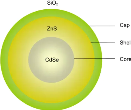
Quantum dots are spherical nano-sized crystals. They can be made of nearly every semiconductor metal (e.g., CdS, CdSe, CdTe, ZnS, PbS), but alloys and other metals (e.g. Au) can also be used (Alivisatos, 1996; Bailey and Nie, 2003; Zheng et al., 2004a). The prototypical quantum dot is cadmium selenide (CdSe). Quantum dots range between 2 and 10 nm in diameter (10 to 50 atoms). Generally, quantum dots consist of a semiconductor core, overcoated by a shell (e.g., ZnS) to improve optical properties, and a cap enabling improved solubility in aqueous buffers (Figure 5).
Figure 5. Schematic representation of a quantum dot. The cadmium selenide core is surrounded by a shell of zinc sulphide. Finally, a cap of silica encapsulates the binary quantum dot.The diameter of quantum dots ranges between 2-10 nm.
Synthesis
In the 1980s traditional lithography-based techniques (a combination of electron beam lithography and etching) were used to make quantum dots. However, these quantum dots are only in the nanometre scale in one dimension. The other two dimensions are limited by the
CdSe ZnS SiO2 Core Cap Shell
resolution of the lithography. In the early 1990s, quantum dots were mainly prepared in aqueous solution with added stabilizing agents. This procedure yielded low-quality quantum dots with poor fluorescence efficiencies and large size variations. From 1993 onwards, the high-temperature organometallic procedure was used for growing quantum dots (Murray et al., 1993). This procedure yields nearly perfect crystal structures and narrow size variations, but the fluorescence is still relatively low. The deposition of a surface-capping layer such as ZnS or CdS was found to dramatically increase the fluorescence properties of CdSe nanocrystals (Hines and Guyot-Sionnest, 1996). The resulting quantum dots are highly hydrophobic and only soluble in nonpolar solvents. The art of quantum dot synthesis is evolving as alternative precursor materials, such as CdO, can be used to prepare high quality CdS, CdSe, and CdTe nanocrystals (Peng and Peng, 2001). In contrast to traditional binary quantum dots, and core/shell nanocrystals, the quantum dots synthesized show excellent quantum yields without an inorganic capping layer. The size of the quantum dot can be controlled by temperature (>300 °C) and period of time, ranging from minutes to hours depending on the desired particle size.
Properties
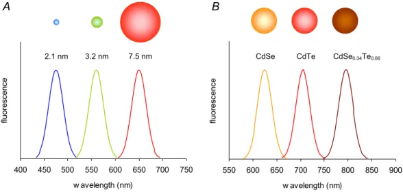
Quantum dots take advantage of the quantum confinement effect, giving these nanoparticles unique optical and electronic properties. A theoretical framework for these properties was already described in 1982 by two research teams in the former Soviet Union (Efros and Efros, 1982; Ekimov and Onushchenko, 1982). Fluorescence semiconductor quantum dots offer advantages in that they have a tunable absorption spectrum, which is very broad, extending from the ultraviolet to a cut-off wavelength in the visible spectrum. Emission is confined to a narrow band and can also be tuned. Absorption and emission characteristics are dictated by size for binary quantum dots or by composition/internal structure independently of size for alloyed semiconductor quantum dots, such as CdSeTe (Bailey and Nie, 2003). When illuminated, smaller binary quantum dots emit shorter wavelength, such as blue, whereas larger dots emit longer wavelength, such as red (Figure 6). Moreover, quantum dots have brighter emission and good photostability.
Figure 6. Optical properties of binary and alloyed quantum dots. Schematic drawings of three CdSe quantum dots with different diameters (A) and three quantum dots (mean diameter ~5 nm) with different composition (B) and their corresponding fluorescence emission spectra. Modified from Bailey and Nie (2003).
400 450 500 550 600 650 700 750 w avelength (nm) fluorescence 2.1 nm 3.2 nm 7.5 nm A 550 600 650 700 750 800 850 900 w avelength (nm) fluorescence
CdSe CdTe CdSe0.34Te0.66