[Año]
Converter for direct use of a deep-freezer on solar PV
Luis Manuel Chaves Costa
Student number: 01903446Supervisor: Prof.dr.ir. Alex Van den Bossche Counsellor: Ali Farzan Moghaddam
Assessor: Vicente Luis Fuster Roig
Master’s thesis submitted in order to obtain the academic degree of Master of Science in Electromechanical Engineering
2 © Copyright Ghent University.
This master thesis contains confidential information and confidential research results proprietary to Ghent University or third parties. It is strictly forbidden to publish, cite or make public in any way this master’s thesis or any part thereof without the express written permission of Ghent University. Under no circumstance may this master thesis be communicated to or put at the disposal of third parties. Photocopying or duplicating it in any other way is strictly prohibited.
Disregarding the confidential nature of this master thesis may cause irremediable damage to Ghent University.
3
Preface
I would like to express my gratitude to the university researcher team for helping me to feel welcomed in the university from the first moment. To my promotor Alex Van den Bossche and Ali Farzan Moghaddam for giving me the necessary help and guidance throughout the project process and to my family and friends for providing to be a great support when it is most need. My most sincere gratitude goes to all of them.
4
Contents
Preface ... 3
Contents ... 4
Abstract ... 5
List of Figures and Tables ... 7
1 Societal constraints ... 9
2 Direct PV operated Freezer ... 11
3 Boost Converter ... 13
3.1 Description and functioning ... 13
3.2 Schematic ... 13
3.3 Layout ... 16
3.4 Circuit ... 17
4 Bridge Converter ... 19
4.1 Description and functioning ... 19
4.2 Schematic ... 19
4.3 Layout ... 22
4.4 Circuit ... 23
5 Processor ... 24
5.1 Description and functioning ... 24
5.2 Schematic ... 25
5.3 Circuit ... 26
6 Measurements ... 27
6.1 Test Methodology ... 27
6.2 Motor Current Test ... 27
6.3 Boost Converter and Bridge Converter Voltage Test ... 31
6.4 Bridge Converter and Motor Waveform Test ... 33
6.5 Bridge Converter No Load Losses Test ... 36
6.6 PV Panel Test ... 38
7 Conclusions ... 39
7.1 Conclusions ... 39
7.2 Future lines of the project ... 40
Appendices ... 41
A. Bill of Materials ... 41
B. Arduino PWM code ... 43
5
Abstract
The Earth's climate has changed throughout history. Most of these climate changes are attributed to very small variations in Earth’s orbit that change the amount of solar energy our planet receives.According to Intergovernmental Panel on Climate Change, IPCC [1] [2], Scientists attribute the global warming trend to the human expansion of the “greenhouse effect” warming that results when the atmosphere traps heat radiating Earth toward space.
On Earth, human activities are changing the natural greenhouse. Over the last century the burning of fossil fuels like coal and oil has increased the concentration of atmospheric carbon dioxide (CO2) due to the industrial activities that our modern civilization depends upon.
The consequences of changing the natural atmospheric greenhouse are difficult to predict, but certain effects seem likely: Loss of sea ice, accelerated sea level rise (based on an assessment report 5 AR5 by IPCC [1] [2]) It can also generate longer, more intense heat waves.
The long-term strategy according to The European Commission [5] “opens a through
debate on how the EU should prepare itself toward the 2050 horizon. Reaching a
climate neutral economy by 2050 is feasible from technological, economic and social
perspective, but it requires deep societal and economic transformations within a generation”.
1. Fully decarbonising Europe’s Energy supply: Large scale electrification of the
energy system coupled with deployment of renewables will decarbonise our energy supply towards 2050 and significantly reduce our dependency on third country suppliers.
2. Embracing clean, safe and connected mobility: Decarbonising the transport
sector by using alternative means of transport, connected and automated driving combined with the roll-out of electric vehicles and enhanced use of alternative fuels.
3. Maximising benefits from energy efficiency: Reducing fossil energy
consumption by close to half between 2005 and 2050.
4. Putting industrial modernisation at the centre of a fully circular economy:
Reaping first mover benefits by modernising existing installations and investing in new carbon neutral and circular economy-compatible technologies and systems.
5. Developing smart network infrastructure and interconnections: A modern
and smart infrastructure, ensuring optimal sector coupling and enhancing regional cooperation, is the cornerstone of the energy transmission and distribution landscape of tomorrow.
6. Reaping the full benefits of bioeconomy and creating essential carbon sinks: Creating natural sinks by developing more sustainable land-use and
agriculture.
7. Tackling remaining CO2 emissions with carbon capture and storage:
Compensating for remaining greenhouse gas emission in our economy an creating negative emissions.
6 Today, society is more and more aware of climate change, however, the increase in globalisation and the increase in the need for resources have more weight on the planet trend than our ideals, so we must consider actions that are in our daily activities to reduce the effect of the current and future situation. Design a converter for direct use of a Deep freezer on solar PV is a tentative in the broader target.
7
List of Figures and Tables
List of Figures
Figure 2.1. Project schematic. ... 12
Figure 3.1. HV9961 typical connection diagram. ... 14
Figure 3.2. Boost Converter schematic. ... 15
Figure 3.3. Basic schematic layout. ... 16
Figure 3.4. Boost Converter layout. ... 16
Figure 3.5. Boost Converter perspective view. ... 17
Figure 3.6. Boost Converter top view... 18
Figure 4.1. IRS2153D typical connection diagram. ... 20
Figure 4.2. IRS2153D basic timing diagram. ... 21
Figure 4.3. Half Bridge Converter schematic. ... 21
Figure 4.4. Half Bridge Converter layout. ... 22
Figure 4.5. Bridge Converter perspective view. ... 23
Figure 4.6. Bridge Converter top view. ... 23
Figure 5.1. Voltage waveform for the motor. ... 24
Figure 5.2. Pulses required to supply the motor. ... 25
Figure 5.3. Arduino Leonardo without headers. ... 26
Figure 5.4. Arduino Leonardo with connections. ... 26
Figure 6.1. Deep Freezer motor. ... 27
Figure 6.2. Deep Freezer motor scheme. ... 27
Figure 6.3. Deep Freezer current waveform in starting up. ... 29
Figure 6.4. Refrigerator motor scheme. ... 29
Figure 6.5. Refrigerator motor nameplate. ... 30
Figure 6.6. Refrigerator current waveform in starting up. ... 31
Figure 6.7. Boost Converter and Bridge Converter Test. ... 32
Figure 6.8. Voltage waveform at the output of the Bridge Converter. ... 32
Figure 6.9. Resistors and universal motor. ... 32
Figure 6.10. Bridge Converter and Deep Freezer waveform test. ... 33
Figure 6.11. Deep Freezer current waveform connected to the circuit. ... 33
Figure 6.12. Deep Freezer voltage and current supplied by Bridge Converter pulses. ... 34
Figure 6.13. Period of Deep Freezer current supplied by Bridge Converter pulses. ... 35
Figure 6.14. Refrigerator current waveform connected to the circuit. ... 35
Figure 6.15. Period of Refrigerator current waveform connected to the circuit. ... 36
Figure 6.16. Bridge Converter no load losses test 1. ... 37
Figure 6.17. Bridge Converter no load losses test 2. ... 37
Figure 6.18. PV panel test. ... 38
List of Tables Table 5.1. Timing and sequence of the pulses. ... 25
Table 6.1. Deep Freezer motor R-L measurements. ... 28
Table 6.2. Refrigerator motor R-L Measurements. ... 30
Table 6.3. Voltage at input/output of Boost Converter and Bridge Converter... 31
8 Table 6.5. Features of pure sine inverters on the market... 38
Table A. 1. Boost Converter BOM. ... 41 Table A. 2. Bridge Converter BOM. ... 42
9
1 Societal constraints
The targets for 2050 are formulated but how to get it in a realistic and cost-effective way? so there is a problem to solve.
Fortunately, there are some facts that will increase the possibilities: the PV panels are cheaper than ever. The residential case is taken as an example. PV panels can be put on the full roof, this over-sizing permits to get about the required electricity even in winter. [7]. The excess energy in summer can be used to store it in heat for the winter. Other solutions use methanol or ammonia to store for a longer time or to be transported. Ultra-light vehicles permit reducing the kWh for mobility.
Particularly, the direct use of PV can be cost effective. In the early stage of photovoltaic panels already pumps worked in sunny periods. Gradually PV was used to inject in the grid and at off grid using batteries. However, a lot of appliances can operate directly on DC without injecting in a grid, nor batteries. According to [8] There are a lot of appliances that use SMPS: switched mode power supplies. They often use a rectifier at the input and can work also well in DC, but not mentioned nor guaranteed: so, we need a label. Some loads such as laptops also store in their own battery. Electric boilers can also be made for DC. Further on, also more industrial processes could be considered: flour mills, wastewater pumps. Also charging vehicles and other emerging applications:
- Refrigerator: a need to store in ice but could be developed. Small items can use Peltier.
- Freezer: if the freezer is well insulated, it can retain for 48-72 hours, could work using the thermal time constant. It is possible to oversize the PV so that a fridge or freezer could be used on/off.
- Compressed air storage: expansion generates cold and power at the same time. It should be changed to sunny periods and it is not well developed yet.
- Air conditioning: ice storage cooling systems, to cover needs in the evening or clouds. It reduces the stress of the grid: at maximal sun the distribution transformers run hot.
The cost of only panels (No inverter, no installation, no interest, no benefit and no maintenance) for private use is 380 €/kWp installed, VAT included [8]. For companies that own large farms, the price of naked PV panels is around 250 €/kWp VAT excluded [8].For private persons the cost of the panels is adapted from Direct use of PV Panels [8], according to [14]: 96€/0.28kWp= 343 €/kW spread over 25 years, without interest, at 1000 kWh/kWp/year and 20% of degradation on average is 343/(1000*0.8*25) = 0.01715 €/kWh. So the art will be to reduce other costs such as mounting and energy storage. There are several cases in which the installations use batteries to store the energy produced. In these cases, the cost of the installation increases, making the idea of installing many projects to take advantage of the energy disappear. A battery of Li-ion type has a cost around 300 €/kWh whereas a Pb-acid has a cost around 150 €/kWh. For 1500 equivalent full charges (EFC) Li-ion, the cost of every charge is 0.2 €/kWh, whereas Pb-Acid is 500 EFC and then 0.3 €/kWh [8].
In the case of the AC grid connection, there are costs of connection, Grid installations and Power plants. If not subsidized and not abnormally taxed energy bill is 0.1-0.3 €/kWh for private use and 0.06-0.15 €/kWh excluded VAT for companies [8]. Apart from that, the grid injection feature is not available at a local or global shutdown, a too high grid voltage, or a (sometimes intentional) frequency deviation.
10 There are some differences in AC power with respect to DC power:
- DC-DC and pulsed converters have a lower B.O.M
- DC-DC have a much higher efficiency than DC-AC inverter which indicates how much power is converted from DC to AC, and with DC-DC there is no need to convert .The no-load consumption of DC-DC can be down to 1W or even lower (e.g. 1.53 mA), and in standby even lower.
The conclusions of the last paragraphs above are the following:
- Battery storage can increase the cost of ownership by a factor 10 compared to naked PV.
- Grid injection has a cost as well as generate problems in case of shutdown or frequency deviation.
- DC use is cheaper and less no-load than first converting to AC. - The Direct PV use is about the cheapest electric energy of today.
11
2 Direct PV operated freezer
Today, there is a tendency to look also at direct use of PV-panels, without injecting in the grid and without storing in a battery. Indeed, some loads such as water heaters are storing themselves at a lower cost than a battery. A lot of people have a few kW of panels. In Belgium the PV panels are usually intended to inject into the grid. However, the grid injection feature is not available at a local or global shutdown, a too high grid voltage, or a (sometimes intentional) frequency deviation. Even if several kW PV is potentially available, it is not possible to operate a freezer that needs only a power of about 50-100 W in the winter from time to time. In the summer more power is required, but there is also more light. The question is what is still possible in December or January, months with the lowest solar productivity. Many instruments work already on DC with Little adaptation.
A "normal" freezer of 230V needs a dedicated circuit to operate well. Some 4.5 kWp installed PV panels, generate still 100 kWh in a normal month of December or January, and the worst month was December 2017, 56.8 kWh, 1.8 kWh/day [15].
A freezer can bridge some 60-h time, so the operation could be possible. In winter an A+++ in good condition it needs 250 Wh/day.
The aim of the Project is to build a single-phase inverter, matching home freezers starting from a normal PV array with some point of attention:
1. Work with low no-load, a DC voltage applied at no-load. 2. Operate without battery.
3. Have enough energy in the DC-link capacitor to get the motor started.
Simple inverters such as square wave and modified sine wave are not good enough for motors. However, some harmonics or imperfections can be tolerated. A modulated DC-link could be an option, creates a rectified sine wave, based on an Arduino.
A full bridge can create an AC with limited PWM from it. Some intelligence of a processor such as an Arduino is useful to create a sine and start and stop in a controlled way. The proposed solution consists of 4 main elements:
1. PV panels: To transform solar energy intro electrical energy with a range of voltages of 150 – 300 V DC.
2. DC/DC Converter: To adapt the Vinput of 150 – 300 V DC to Voutput of 300 V DC with a current Iout between 1.66-2 A working with a frequency of 40 kHz. An electrolytic capacitor that store enough energy to get the motor started is included in the converter circuit.
3. Bridge Inverter: To create an AC wave based on Arduino with a particular type of timing for pulses. The voltage and PWM edge frequency are limited in order not to blow up the internal power supply for the control of the freezer. The harmonics in the current are limited not to damage motor.
4. Deep-Freezer motor: AC motor that needs a supply of about 230V fundamental voltage at the input of the circuit.
12
Figure 2.1. Project schematic.
The project is a solution to reduce the global problem of climate change in a cost-effective way using renewable energy.
The differences between the proposed solution and others are the following:
- DC-link instead of AC link. This fact reduces no-loads, have a lower B.O.M and have a much higher efficiency.
- No battery in the system. Reduce the price of the installation, approximating the target of how to get it in a realistic and cost-effective way.
- An electrolytic capacitor to have enough energy in the DC-link to get the motor started. 0.3-0.5 seconds to start and if the solar energy gives 40 W the circuit could continue to work properly.
The same project can be used with the corresponding variants for other receptors in DC, setting a start in this field.
Additionally, apart from the electrical requirements necessary to power the Deep Freezer, it is also necessary to take into account the thermal aspect that keeps the products at the right temperature. The calculations of thermal inertia are the following:
- As starting point, 9 operation hours are considered for a COP Coefficient Of Performance of 3-4, an A+++ freezer might need 0.3 – 0.4 kWh/day at that time of the year. 400/9 = 44.4 W, it might turn almost continuous.
- Taking into account the converter efficiency and more losses it might need 50– 60 W.
- 0.4 kWh/day at COP = 3 is 1.2 kWh heat storage over one day. 24 – 9 = 15h to cover. 1.2*15/24 = 0.75 kWh in cold to store for one day. It is 2.7 MJ.
Following the research of Inorganic Salt Hydrate for Thermal Energy Store [13]:
- 21.2% NaCl gives -21.2 melting temperature 222 kJ/kg. For pure water 334 kJ/kg so probably at -16ºC some 250 kJ/kg. With the results above, 2.7/0.25 = 10.8 kg. - Sodium chloride 15% is some 1.12 kg/l. 10.8/1.12 = 9.64 l, close to the cooling
heat exchange area.
More time can be obtained with more litres but also the food adds to the thermal inertia as well.
13
3 Boost Converter
3.1 Description and functioning
Some converters need to convert a DC voltage in another DC voltage without galvanic separation, also called “choppers”. Depending on the application, very different output ripples are allowed. For power supply applications it is usually required that a low ripple of 1% or lower is obtained. Other applications like DC machines, batteries, galvanization, welding with DC, allow a lot of DC voltage ripple or current ripple could be accepted. There are different choppers, depending on the necessities of the project:
1. Single Quadrant choppers:
a. Buck converter: to convert an input voltage to a lower output voltage, with a higher output current. It is also called “step-down converter”. b. Boost converter: the output voltage is always at least as much as the
input voltage. It is also called “step-up converter”.
c. Buck-boost converter: to obtain a negative voltage from a positive one. It is also called “Inverting converter”.
d. Cúk converter: to invert the voltage and allow a wide range of output voltage from zero to infinite. It has the advantage that the currents in input and output capacitor are smooth because of the presence of an inductor on both sides.
2. Two Quadrant choppers:
Two quadrant converters can have two types of topologies: two current directions and one voltage or two voltage directions and one current.
3. Four Quadrant choppers:
Four quadrant converters have two possible current directions and two voltage directions. It is also called a full-bridge DC-DC converter.
The application of the boost converter in the project is to boost the voltage from the range 150 – 300 V DC to 300 V DC with an output current of 1.66 – 2 A working with a frequency of 40 kHz. The design of the boost converter contains an electrolytic capacitor to supply the energy that is required to get the motor started.
3.2 Schematic
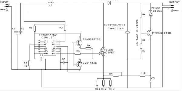
The development of this converter has been carried out based on this scheme.
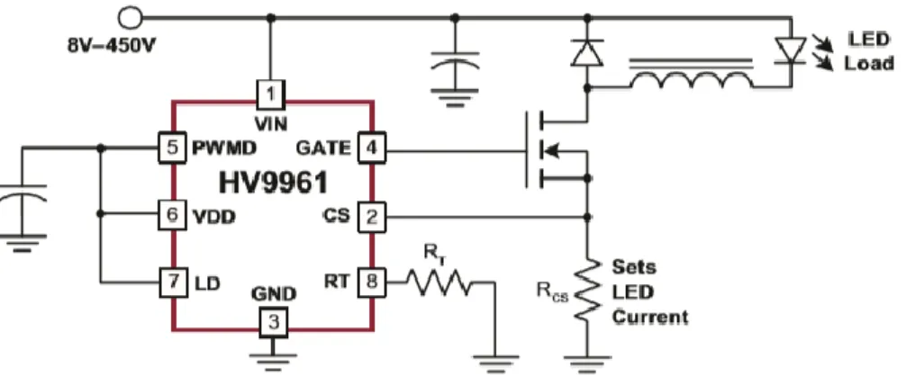
The current generated by solar panels supply the DC motor through the MUR460+ Power Diode, which is controlled by the IPW60R037P7 Power MOSFET, that is activated by the HV9961 NG-G Integrated Circuit which is commonly used as Led Driver.
Integrated Circuit HV9961 Functional Description
The HV9961 [12] is an Average-Current mode constant-current control LED driver IC operating in a constant Off-time mode. This IC is used to improve current accuracy and regulation for many applications.
14 Peak current control is used to regulate the boost converter’s output current. The full inductor current signal is unavailable for direct switch current sensing across the sense resistor at the ground path in the low side switch boost converter when the control switch is at the ground potential because the switch is turned off. The peak current is detected in the switch and controlling the average inductor current is usually implemented by level translating the sense signal from +VIN.
The HV9961 uses a proprietary control scheme that allows fast and accurate control of the average current in the boost converter by sensing the switch current only. The LED current is independent of the variation in inductance, switching frequency or output voltage. The constant off-time control of the boost converter is used for stability and improving the LED current regulation over a wide range of input voltages.
Figure 3.1. HV9961 typical connection diagram.
The timing resistor connected between RT and GND determines the off-time of the gate driver, Toff (µs).
The current through the switching MOSFET source is averaged and used to give constant-current feedback. This current is detected with a sense resistor at the CS pin. The feedback operates in a fast Open-Loop mode.
The duty-cycle range of the current control feedback is limited to D ≤ 0.75. a reduction in the LED current may occur when the desired LED string voltage Vo is greater than 75%
of the input voltage VIN of the HV9961 LED driver. In our application as boost converter,
this limitation is no problem for the considered input voltage and output voltage range. Reducing the target output LED string voltage Vo below Vo(min) may also result in the loss
of regulation of the LED current. This condition, however, causes an increase in the LED current and can potentially trip the short-circuit protection comparator.
The short-circuit protection comparator trips when the voltage at CS exceeds 0.44V. When this occurs, the short-circuit gate off-time is generated, of 400 µs, to prevent the staircasing of the inductor current and, potentially, its saturation due to insufficient output voltage.
In the case of the Linear Dimming, when the voltage at LD falls below 1.5 V, the internal 275 mV reference to the constant current feedback becomes overridden. As long as the current in the inductor remains continuous. When the voltage at LD falls below 150 mV, the gate output becomes disabled. The gate signal recovers when it exceeds 200 mV.
15 This linear dimming is not used as the gain of it has a wrong sign to be used as a feedback.
The Gate output is used to drive an external MOSFET. It is recommended that gate charge of the external MOSFET be less than 25 nC for switching frequencies ≤100 kHz and less than 15 nC for switching frequencies >100 kHz. For that, reason there are added an NPN and a PNP voltage follower transistor. It is also as the gate current output is quite low.
Due to the fast open-loop response of the average-current control loop of the HV9961, its PWM dimming performance nearly matches. The rising and falling edges are limited by the current slew rate in the inductor. The first switching cycle is terminated upon reaching the 275 mV or the voltage level at CS. The circuit is further reaching its steady state within 3-4 switching cycles regardless of the switching frequency. The PWM dimming feature is not used as it modulates with a lower frequency.
Feedback Description
The circuit is based on a constant current control using the HV9961 IC.
The feedback could be controlled by the Linear Dimming input, but the gain has opposite polarity to be used as feedback, so an amplifier would have to be added to work correctly, which would generate more consumption than one used by the IC itself. The CS pin has the right polarity for the control for feedback.
After filtering, the voltage feedback using a PNP transistor adds voltage to the voltage coming from the shunt and influences the control of the CS pin of the IC. The transistor circuit has a high gain to keep the voltage output. The operating mode of the IC is described in the previous IC functional description.
Some more details: the PNP transistor has a voltage divider at the base, and a Zener diode at the emitter. A Zener diode of 7.5V has a voltage drop with PTC effect (Positive Temperature Coefficient) which is compensated by the base emitter NTC effect of the transistor. A current limiting resistor is put in the collector of the transistor.
16
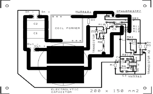
3.3 Layout
The layout of the boost converter has been made based on the converter scheme, taking into account the size of the components as well as reduce as much as possible the combined problems of the parasitic inductance, the inductive mutual coupling, the parasitic capacitance. The plan followed to develop the layout is the following:
Figure 3.3. Basic schematic layout.
The idea of this basic layout is:
- Narrow the distance between copper tracks to reduce parasitic inductance. - Separate components that are part of power tracks from integrated circuits used
for control, avoiding disturbance.
- Use of wide tracks to reduce the losses and facilitate heat dissipation in power tracks.
- Set the input and the output of the circuit very close to obtain a short mass path, reducing inductance.
- A single layer is preferred in a prototype realisation.
17 Analysing the circuit implemented, the considerations proposed above are largely observed:
- The dimensions of the components significantly influence the distribution of the entire circuit: the capacitors and the inductor at the circuit input as well as the electrolytic capacitor are almost half of the full circuit.
- A series of values for widths of the tracks are proposed depending on the part of the circuit: 5 mm for power tracks, 0.7 mm for the connections of the integrated circuit and 1 mm for the rest of the tracks. In the case of de electrolytic capacitor, enough surface of cooper is located under the capacitor to facilitate the connexion and the power distribution.
- The inputs/outputs are next to low impedance elements such as capacitors. - Power tracks are separated from integrated circuit.
- The power MOSFET is at the side of the circuit to facilitate its heat evacuation. The Power MOSFET is coupled with a heat sink to perform this action more effectively.
- Resistors with 0 ohms values are used to avoid contact from different paths. At a low number this is easier and cheaper than double layer circuit and could be automatic inserted.
- Still after this first prototype, the lay out could be made more compact, but having some space was also easier to measure and debug.
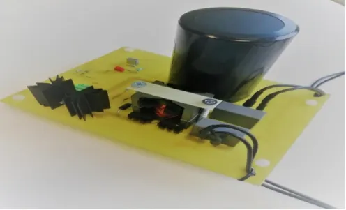
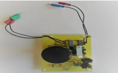
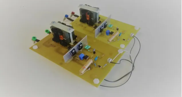
3.4 Circuit
The circuit assembly has been done manually in the power electronic lab of the department of Electrical Energy, Metals, Mechanical Constructions and Systems of Ghent University.
18
19
4 Bridge Converter
4.1 Description and functioning
A full H-bridge inverter uses active switching components in a configuration that can creat an AC voltage.
The basic circuit consist of four active switching devices such as MOSFETs, Bipolar transistor or thyristors, IGBTs, associated to drive circuits. The switching waveform could be either square or sinusoidal and while square wave is simpler to implement, it has more harmonic content. Some reaction on internet report to power a freezer from a “modified square wave”, what some people also call “modified sine wave” although it does not look like a sine [16].
Motors, such as refrigerator motor, pumps, fans etc will use more power from the inverter due to lower efficiency. Most motors will use about 20% more power. This is because a fair percentage of a modified sine wave is higher frequencies – that is, not 60 Hz – so the motors cannot use it [16].
The intention in this work is to create a waveform that is somewhat better than a modified square wave, but not with a PWM frequency of more than 10 kHz that could overheat the EMC filter of an internal power supply for the temperature control and interface to the user.
The application of the full bridge converter in the project is to create a PWM on a processor, Arduino, that control the driver circuit. It needs also to provide some intelligence what to restart after some time if a first start does not succeed. The active switching devices used for the bridge are MOSFETs in the high-power part of the circuit. The basic operation involves switching one pair of transistors at a time for one half cycle of the control waveform and the other pair during the other part of the waveform. The control strategy uses the pulse width modulation (PWM) signal to switch the transistors on each leg simultaneously as a pair.
4.2 Schematic
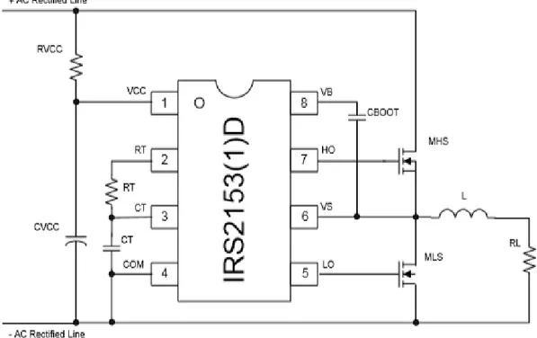
The development of this bridge converter has been carried out based on the scheme of [11].
The voltage at the input comes from the boost converter. The Integrated Circuit IRS2153DPBF is supplied by this level of voltage and active the switching MOSFETs, IPA60R180P7S, controlled by Arduino Leonardo, transforming the DC signal to AC, which is required by the induction motor.
Integrated Circuit IRS2153DPBF Functional Description
The under-voltage lockout mode (UVLO) is defined as the state the IC is in when Vcc is below the turn-on threshold of the IC. This UVLO is designed to maintain an ultra-low supply current of less than 170 µA, and to guarantee the IC is fully functional before the high and low side output drivers are active. During UVLO, the high and low-side driver outputs HO and LO are both low.
The typical Connection for the supply voltage of the IC is on Figure 4.1. The start-up capacitor (Cvcc). charged by current through supply resistor Rvcc minus the start-up
20 current drawn by the IC. This resistor is chosen to provide sufficient current to supply the IC from the de DC bus. Cvcc should be large enough to hold the voltage at Vcc above the UVLO threshold for one half cycle of the line voltage as it will only be charged at the peak.
Figure 4.1. IRS2153D typical connection diagram.
The internal bootstrap MOSFET and supply capacitor (CBOOT) comprise the supply
voltage for the high side driver circuitry. This only turns on when LO is high. To guarantee that the high-side supply is charged up before the first pulse on pin HO, the first pulse from the output drivers comes from the LO pin.
The normal operating mode is once the Vccuv+ threshold is passed, the MOSFET M1 opens, RT increases to approximately Vcc (VCC-VRT+) and the external CT capacitor starts
charging. Once the CT voltage reaches VCT- (about 1/3 of VCC), established by an internal
resistor ladder, LO turns on with a delay equivalent to the deadtime (DT). Once the CT voltage reaches VCT+ (approximately 2/3/ of VCC), LO goes low, RT goes down to
approximately ground (VRT-), the CT capacitor discharges and the deadtime circuit is activated. At the end of the deadtime, HO goes high. Once the CT voltage reaches VCT-, HO goes lowVCT-, RT goes high againVCT-, the deadtime is activated. At the end of the deadtimeVCT-, LO goes high and the cycle starts over again.
In the case of the project, the VC voltage is controlled by Arduino Leonardo instead of the RT feedback. Figure 4.3 shows the scheme used for the requirements of the project. The functional description of the Arduino is described in the chapter 5: Processor.
21
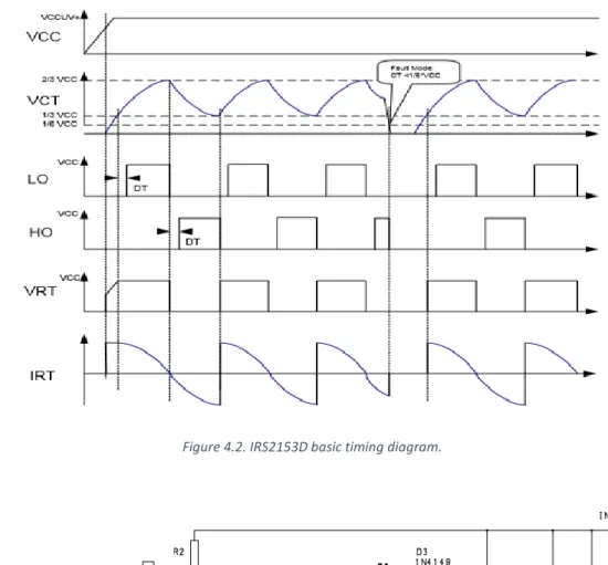
Figure 4.2. IRS2153D basic timing diagram.
Figure 4.3. Half Bridge Converter schematic.
Current Protection
If the CT is pulled down below VCTSD (approximately 1/6 of VCC) by an external circuit, CT
does not charge up oscillation stops. LO is held low and the bootstrap MOSFET is off. Oscillation will resume once CT is able to charge up again to VCT-. This feature is used
to protect the bridge from overcurrent by pulling down CT lower than 1/6th of the supply,
22 The schematic contains all the components that are necessary to have the full circuit working properly including protection and feedback system.
An interesting feature of the circuit is that it can operate with about 1.5mA supply. So a design could be made without an internal switched mode power supply.
The power supply resistor is chosen quite low to allow also an operation at a low DC value.
4.3 Layout
The layout of the bridge converter has been made based on the converter scheme of
Figure 3.2. Basic schematic layout taking into account the size of the components as
well as reduce as much as possible the combined problems of the parasitic inductance, the inductive mutual coupling, the parasitic capacitance. The plan followed to develop the layout has been the same that for the boost converter.
Figure 4.4. Half Bridge Converter layout.
Analysing the circuit implemented, the considerations proposed above are largely observed:
- The dimensions of the components significantly influence the distribution of the entire circuit: In this case the coil former for the inductor and the input and output for the circuit are together. The Arduino is separated from the circuit, using its own input.
- A series of values for widths of the tracks are proposed depending on the part of the circuit: 5 mm for power tracks and 1 mm for the rest of the tracks.
- The inputs/outputs are next to high impedance elements such as coils at the input of the circuit and next to power components such as MOSFETs and diodes, all components in the same zone of the circuit.
23 - Power tracks are separated from integrated circuit.
- MOSFETs having enough space to facilitate its heat venting. The MOSFETs is coupled with a heat sink to perform this action more effectively.
- Resistors with 0 ohms values are used to avoid contact from different paths.
4.4 Circuit
The circuit assembly has also been done manually at the power electronics lab belonging to EELAB, a part of the department of Electrical Energy, Metals, Mechanical Constructions and Systems of Ghent University.
Figure 4.5. Bridge Converter perspective view.
24
5 Processor
5.1 Description and functioning
The entire circuit will be a DC-link between the solar panels and the induction motor. A PWM signal is required by the AC motor. This PWM signal is generated by an Arduino Leonardo.
The Arduino Leonardo is a microcontroller that has 20 digital input/output pins, of which 7 can be used as PWM outputs and 12 as analog inputs. Each of these pins can be used as an input or output, using the functions pinMode(), digitalWrite(), and digitalRead() in the Arduino software. The Arduino digital pins give 5V when the pin is turned “HIGH” or 0V when “LOW” and the output is a square wave signal. The main parameters that are associated with PWM are the followings:
- TON (On Time): It is the time when the signal is high. - TOFF (Off Time): It is the time when the signal is low. - Period: It is the sum of on time and off time.
- Duty Cycle: It is the percentage of time when the signal was high during the time period.
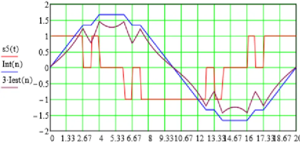
The application of the Arduino is to create a PWM wave at the output from a pulse signal. The derivation of it was not considered to be a task of the thesis and was delivered by the promotor. The pulse signal is based on the use of a waveform shown in the blue curve in Figure 5.1. voltage waveform for the motor. The blue wave is the integral of the red voltage supplied to the motor. The brown curve is the same integral where some back electromagnetic field (emf) is subtracted and amplified, this in order to evaluate what type of current shape could be expected. The red waveform is used to create the PWM angles. With this type of square wave, the harmonics 5th and 3rd all multiples of
third were eliminated. The calculation of these curves is based on series of sines and cosines, applied in Mathcad with the concept of PWM to obtain the square wave.
Figure 5.1. Voltage waveform for the motor.
The square waveform is obtained in Arduino software from the series of pulses that is generated from the following combination of output pins in Table 5.1. Timing and
25
Table 5.1. Timing and sequence of the pulses.
NUMBER OF TIMING START TIMING PERIOD (ms) END TIMING PERIOD (ms) OUTPUT LEFT-RIGHT LEGS PULSE 1 0 2.67 1-0 Long 2 2.67 3.33 0-0 Short 3 3.33 4 1-0 Short 4 4 6 0-0 Long 5 6 6.67 0-1 Short 6 6.67 7.33 0-0 Short 7 7.33 12.67 0-1 Long 8 12.67 13.33 0-0 Short 9 13.33 14 0-1 Short 10 14 16 0-0 Long 11 16 16.66 1-0 Short 12 16.66 17.33 0-0 Short
The period of 20 ms is obtained in Arduino by the following form shown in Figure 5.2.
Pulses required to supply the motor. As it is observed, waveform is designed for a AC
300 V voltage at the output.
Figure 5.2. Pulses required to supply the motor.
5.2 Schematic
The Arduino is an integrated circuit, so the design comes from the factory. The circuit scheme corresponds to Figure 5.3 Arduino Leonardo Schematic. The main operation of the microcontroller is described in the previous section. As information to add, it must have an external power supply of 7-12 V. The code is stored in the memory of the microcontroller.
In the case of the project, the following inputs/outputs are used: - External power input with a 12 V power supply.
- Connection to the two GND pins that connect with both Half Bridges.
26
Figure 5.3. Arduino Leonardo without headers.
5.3 Circuit
The Arduino used in the project with the respective connections is as follows:
27
6 Measurements
6.1 Test Methodology
For this section, a methodology has been stablished to test the complete circuit in stages: 1. Motor Current Test.
2. Boost Converter and Bridge Converter Voltage Test. 3. Bridge Converter and Motor Waveform Test.
4. Bridge Converter No Load Losses Test 5. PV Panels Test
6.2 Motor Current Test
Deep Freezer Motor
The motor for which the converter is designed is a Deep Freezer motor without a starting current appearing on nameplate. To analyse the current demanded by the motor, the internal motor circuit has been analysed a measured. The scheme in which it is based on, contains two inductances in parallel to a capacitor of 5 µF and this circuit in parallel with a PTC thermistor, used to start the motor. The scheme is shown in Figure 6.2. Deep
Freezer motor scheme.
Figure 6.1. Deep Freezer motor.
28 The measurements obtained to determine the impedances of the circuit depending on the frequency were carried out with the oscilloscope RIGOL DS1104B. The results were as follows:
Table 6.1. Deep Freezer motor R-L measurements.
R-L SERIES MEASUREMENTS f (Hz) L1 (mH) R1 (Ω) L2 (mH) R2 (Ω) L1+ L2 (mH) R1+ R2 (Ω) 20 255.3 23.3 482 50.4 611.9 61.9 50 221.3 33.4 447.7 55.9 597.2 82.6 60 211.4 36.2 445.1 60.4 591.1 88.6 100 122.2 45.8 426.3 78.5 558.9 112.4 200 117.5 47.3 389.9 121.2 502.8 167.3 500 105.3 99.3 349.1 240.4 445.9 316.6 1K 91.3 184.3 303.7 433.6 385 559.4 2K 86.7 360.1 268.4 864.5 340.1 1098.5 5K 57 848 204.2 2554.3 260.6 3256.1 10K 43.8 1656.6 174.7 6937.9 223.6 8911.5 20K 30.3 3409.2 68.7 27081 87.3 35182 50K 16.9 8504 -32.7 10341 -35 11086
Using the frequency at 500 Hz as the basis for higher harmonics, The capacitor gets a low impedance and the impedance gets mainly inductive. L1 and L2 take the values of 105 mH and 349.1 mH respectively, so the parallel inductance is 80.7 mH, assuming 70 mH due to internal motor factors. For 300 V DC a current of 4.3 A/ms is expected, The calculation for 50 Hz was done using the web calculator Symbolab. At 50 Hz the impedance would be for 20 ohm PTC:
𝑍𝑚𝑜𝑡𝑜𝑟 = 1 1 0.2213 𝑥 314𝑖 + 33.4+ 1 0.4477 𝑥 314𝑖 + 55.9 + 1 314𝑖 𝑥 5 𝑥 10−6+ 1 20 = 23.250747 + 46.46382𝑖
The equation could be re-inserted to correct for tha PTC value:
\frac{1}{\frac{1}{0.2213\cdot 314\cdot \:i+33.4}+\frac{1}{0.4477\cdot 314\cdot \:i+55.9+\frac{1}{314\cdot \:i\cdot 5\cdot 10^{-6}+\frac{1}{20}}}}
230 𝑥 √2
|23.25+46.46𝑖|= 6.26085 𝐴 𝑝𝑒𝑎𝑘
Also, a real starting current test is done. It is much higher than expected from impedances, the reason is that the RLC meter measures at a low amplitude of about 1V. For high current, the inductive paths are saturated. If one expands a period, one can recognize that the current is almost triangular, which confirms the saturation effect. To see the real current that the motor demands, it is connected to grid and analysed the waveform obtained in the oscilloscope. The graph is contained in Figure 6.3. Deep
29
Figure 6.3. Deep Freezer current waveform in starting up.
Taking into account the scale in which the graph is, a peak at starting up is observed that decreases as the motor operation stabilizes. This peak is 3 divisions of 200 mV each, 600 mV in total. Using a current transformer of 12.5A/5A through a 0.1 Ω resistor, the peak current obtained is 15 A, 15A and 230V results in (15//2^0.5) *230= 2440 VA. This is a very big value for a motor that uses a power typically between 40 and 100W. If a sine wave inverter is used for example a nominal apparent power of 1000VA is needed with a factor 2.5 overload capability. This result corresponds to a typical no-load loss between 10 and 20 W for sine wave inverters. This no-load loss is higher than the average consumption of an A+++ freezer of today.
Analysing the duration of the transitory state of the wave, it takes 11 periods of 50 ms each, so the Boost Converter must supply enough power for the start for a time of 550 ms.
Refrigerator Motor
Additionally, to see the influence of the peak of current in the start-up of the motor, another motor of less consumption, a refrigerator motor, with the following nameplate has been tested. In this case, the motor scheme does not have a capacitor, so it differs completely from the previous motor in terms of waveform and consequently in type of consumption.
30
Figure 6.5. Refrigerator motor nameplate.
The measurements obtained to determine the impedances of the circuit depending on the frequency were carried out with the oscilloscope RIGOL DS1104B. The results were as follows:
Table 6.2. Refrigerator motor R-L Measurements.
R-L SERIES MEASUREMENTS R-L PARALLEL MEASUREMENTS
f (Hz) R1+ R2 (Ω) L1+ L2 (mH) f (Hz) R1+ R2 (Ω) L1+ L2 (mH) 20 66.9 274 1k 6000 173.9 30 68.9 254 2k 10740 165.7 40 70.6 244 3k 13500 161.7 50 66.9 201.7 4k 15400 159 60 67.9 199.2 5k 16800 157 70 69.1 197.3 6k 18000 155.7 80 69.9 196.2 7.2k 19400 154.8 90 71 195.2 8k 20200 154.6 100 72.4 193.1 9k 21200 154.9 150 83.7 188.7 10k 22200 155.8 200 89.6 187.2 20k 31400 225.1 250 85.5 184.9 30k 35000 224.5 300 95.5 182.9 40k 28000 -99 400 107.8 179.7 50k 18400 -126 450 114.0 178.3 100k 10820 -268 500 120.4 177 600 133.4 174.7 750 154 172 Rdc (Ω) 17.8 800 161.2 171.2 900 176.2 169.2
In this case, directly the real current that the motor demands have been analysed. It is connected to grid and analysed the waveform obtained in the oscilloscope. The graph is contained in Figure 6.6. Refrigerator current waveform in starting up.
31
Figure 6.6. Refrigerator current waveform in starting up.
Taking into account the scale in which the graph is, a peak at starting up is observed that decreases as the motor operation stabilizes. This peak is 2.5 divisions of 200 mV each, 500 mV in total. Using a transformer of 12.5/5 through a 0.1 Ω resistor, the peak current obtained is 12.5 A, so a higher starting current of 12.5 A peak is obtained.
Analysing the duration of the transitory state of the wave, it takes 5 divisions of 100 ms each, so the Boost Converter must supply enough power for the start for a time of 500 ms. Note that this is a smaller, table type refrigerator, so that it is normal that the starting current is smaller than the freezer.
6.3 Boost Converter and Bridge Converter Voltage Test
To test the operation of the circuit, the first test was carried out with variable resistors of up to 296 Ω and 1.4 A each one of them in series to an Universal Motor of 0.4 A. The results at the Inputs and outputs of both circuits in the range of high voltage (From 220 V DC at the input of the Boost Converter to 300 V) are shown in the following table:
Table 6.3. Voltage at input/output of Boost Converter and Bridge Converter.
VINBC DC (V) VOUTBC DC = VINHB DC (V) VOUTHB AC = VINLOAD AC (V)
225 286 230
249.3 287 230
276 287 230
293.5 299 239
297 303 245
Viewing the data sheet of the ALS70A512MF400 5100 uF electrolytic capacitor, the ripple current data shows that it can supply 14 A at 100 Hz (10 ms) and 22.5 A at 10 kHz (0.1 ms). Two units in parallel are required to satisfy the high current in the start-up. The voltage waveform is shown in oscilloscope through a factor of x50.
32
Figure 6.7. Boost Converter and Bridge Converter Test.
Figure 6.8. Voltage waveform at the output of the Bridge Converter.
33
6.4 Bridge Converter and Motor Waveform Test
The objective of this test is to prove that the pulses provided by the Bridge Converter, generated by the controller, Arduino, are adequate to power the motor.
Figure 6.10. Bridge Converter and Deep Freezer waveform test.
As seen in the previous image, the waveform at the output of the power MOSFETs at a voltage suitable for supplying the motor, 205 V AC, is analysed. As in the previous section, an analysis of the waveforms demanded by both motors is performed.
Deep Freezer Motor
34 Connecting the motor to the circuit, it is observed that the current waveform demanded by the motor has a not very sinusoidal shape but that is repeated in each period and therefore throughout the permanent regime. Some important reasons are due to the number of harmonics the system contains and also due to the type of scheme that the Deep Freezer Motor has. The harmonics are more visible as the reactive current of the motor is compensated by the capacitor and that the motor is tested at no-load.
Figure 6.12. Deep Freezer voltage and current supplied by Bridge Converter pulses.
Note that in Fig 6.12, the current is inverted, but it is better visible in this way. In a qualitative way, the current waveform seems a sequence of triangles, the typical deviation from the fundamental can be estimated at 1.2 divisions peak-peak or triangles of 0.6 deviations peak.
The rms of the harmonics would be 0.6/30.5 = 0.346 A. In that case the PTC resistor has
a high value and could be neglected for harmonics.
𝑍𝑚𝑜𝑡𝑜𝑟 = 1 1
0.1053 𝑥 314𝑖 + 99.3+
1
0.349 𝑥 314𝑖 + 240.4 +314𝑖 𝑥 5 𝑥 101 −6
= 250.72𝑖 + 71.06
For the estimated rms harmonic current, the additional losses would be:
71.06 𝑥 (0.346 𝐴)2= 8.51 𝑊
Close to the nominal operation, the impedance could be lower as there is more flux, So, the output inductor of the bridge can result is a significant reduction of the current ripple.
35
Figure 6.13. Period of Deep Freezer current supplied by Bridge Converter pulses.
As can be seen in Figures 6.12 and 6.13, the pulses with the highest peak of the motor current coincide with the short duration pulses provided by the Bridge Converter. More narrowly in amplitude, the rest of the motor current peaks coincide with the long-lasting pulses provided by the Bridge Converter.
As conclusion, the choice of this type of generated pulses is good enough to supply the motor. The fact that no capacitor is put at the output saves a lot of no-load losses in the inverter, so that finally the total power delivered by the PV during a day is lowered by the fact that the no-load loss of the inverter is reduced.
Refrigerator Motor
36
Figure 6.15. Period of Refrigerator current waveform connected to the circuit.
Connecting the motor to the circuit, it is observed that the waveform demanded by the motor is closer to a sinusoidal shape in comparison with the previous motor. That is repeated in each period and therefore throughout the permanent regime. Some important reasons are that the refrigerator motor has no capacitor in the auxiliary phase, so the operation contains also a lot of magnetising current, and the motor was still in a working refrigerator, so contains more active current than the freezer one.
As it is observed, the graph shown corresponds in practice with Figure 5.1. Sine and
square waveform for the voltage of the motor. It can be concluded based on the previous
comparison that the type of waveform that is applied by Arduino obtains sufficient good results.
6.5 Bridge Converter No Load Losses Test
The objective of this test is to analyse the no load losses of the Bridge Converter. To perform this test, the Bridge Converter was connected to a power supply through a low-value resistor of 100 Ω to obtain a no-load current at the output of the bridge converter.
The tests performed for different voltage values are as follows:
Table 6.4. No load losses test.
Parameters Test 1 Test 2
VIN (V DC) 150 300 VOUT (V AC) 106 243 I100Ω (mA) 4.1 8.7 ∆V100Ω (V DC) 0.4 0.9 PIN (W) 0.615 2.61 P100Ω (W) 0.0016 0.0078 P68KΩ (W) 0.2978 1.2574
37
Figure 6.16. Bridge Converter no load losses test 1.
Figure 6.17. Bridge Converter no load losses test 2.
As can be observed in the previous results, most of the losses are due to the input resistances of 68 kΩ before the IC, which has a 15 V DC supply.
The losses due to IC, MOSFETS, diodes and other components of the circuit components are very small compared to the power losses at the 68k resistances. The power losses fit the analysis done previously.
To analyse whether these losses are within the usual ranges for inverters, no load losses for various inverters on the market are analysed [17], [18], [19]. These are pure sine
38 inverters, which are the inverters for which are most of the devices that require an inverter are designed [16]. These values are shown in the following table:
Table 6.5. Features of pure sine inverters on the market.
Model No Load Current (A) DC Input Voltage (V) Rated Power (VA) Surge Power (VA) No Load Losses (W) AIMS POWER PWRIG150024120S 0.65 24 1500 3000 <15.6 COTEK SP-2000-224 1 24 2000 3500 <24 COTEK SP-1000-224 0.8 24 1000 1750 <19.2 6.6 PV Panel Test
The objective of this test is to prove that the entire circuit performances properly to supply the Motors.
The configuration used to power the circuit is 2 strings of 6 panels/string. The test was carried out twice with different weather conditions depending on the area.
For a sunny day, this configuration of panels with some grade of degradation obtained a Power of 700 W and 225 V so the motors can be started with that power. For a configuration of 1 string of 6 panels, the power obtained was 350 W with which the motors cannot be started but can keep the operation mode in permanent regime.
In the case of a cloudy day, the configuration of 2 strings and 6 panels/string obtain a power between 70 W and 360 W. This Power is not enough to start but to keep the operation mode in permanent regime of the motors.
Figure 6.18. PV panel test.
The figure shows that the refrigerator motor works with the 2 strings and 6 panels/string with 700 W obtained.
39
7 Conclusions
7.1 Conclusions
The system was designed to be able to work on a PV panel array without batteries nor grid connection. This means that a voltage level conversion is needed (DC/DC) and an inverter. The not used energy may be stored in electric boilers or other apparatus that can work “as and when the sun shines). To cover also the night some thermal inertia might has to be added, but some manufacturers claim 60h autonomy.
The starting power for conventional freezer is in the order of 2000VA, where the steady state is between 40-100W, Additional capacitors were added to bridge the start at a limited power level, to get an easier start in the morning.
The system does not need batteries, so the price of the installation is lower, than systems with battery, may be even compared to grid electricity. It can be seen as an emergency operation or continuous use. Indeed, in the conventional situation, during a long grid shutdown, the food in it may be lost. Refrigerators have much less thermal inertia, and will still require batteries
The use of the used pulse with modulated waveform has the advantage of reducing the 5th and all multiples of 3th harmonic of the voltage wave, having a quite low harmonic
current as a result, having a waveform with higher quality and less losses than a simple modified square wave.
The circuit does not generate an overvoltage spike when the motor is disconnected due to the freewheel diodes and the large electrolytic capacitor in the topology. A voltage spike at disconnecting the motor could damage the internal voltage supply for temperature control and display.
The project was challenging as an actual peak current of 15 A peak, was observed, which is much more than extrapolated from the small signal impedance and what is available on internet. The peak kVA is about 40 times higher than the typical steady state current, which is unusual.
Due to this high starting VA and also W, as it is mainly resistive the original design had to be adapted to cope with it. This means that the electrolytic capacitors are the highest cost in the BOM. A 4000-5000 µF capacitor 400V in obtained in a single or multiple parallel costs about 50€. But the life time might be much longer than a battery based system
The System needs thermal storage to maintain the Deep Freezer temperature between -10ºC and -15ºC.
This project is a step-in letting appliances work directly from PV panels. A freezer needs more Wh/day in summer than in winter, so it is a candidate to be supplied directly from grid. As the electricity direct from PV panels without storage nor grid connection is the cheapest source of energy today, it might stimulate renewable energy, while having negligible CO2 emissions and the potential to be cheaper at the same time.
The same project can be used with the corresponding variants for other appliances, setting a start to supply them with direct solar energy using PV Panels. The system can also use a battery voltage and draw less starting current from it.
40 In the case of developing countries, where the electrical grid system is not as robust and reliable as it is in developed countries, this project allows solar resources to be used without the need to be connected to the grid.
The global grid in developed countries is very robust, so most of electrical receptors are designed to work connected to the grid.
7.2 Future lines of the project
Improve circuit design to reduce spaces, interference, to facilitate heat transfers and increase circuit performance.
If a number of appliances are tested some may need less starting current. A variable frequency start takes much less starting current, but then the whole control circuit has to be replaced, and a much higher DC link might be needed.
It is possible to carry out projects of the same type with different appliances to increase the viability of this type of solutions.
41
Appendices
A. Bill of Materials
Boost Converter
Table A. 1. Boost Converter BOM.
BOOST CONVERTER 2 x ELECTROLYTIC CAPACITOR UNITS COMPONENT MAIN VALUE NAME IN
CIRCUIT
ITEM CODE 4 CONNECTORS IN/ OUT +/-
2 CAPACITORS 10 uF C1, C2 C4AQLBU5100A1XK
1 FERRITE
CORE
PQ 40/40 U1 B65883A0000R097
1 COIL FORMER PQ 40/40 U1 B65884E0012D001
1 DIODE D1 MUR460+ 1 ZENER DIODE 7.5 V ZD1 BZX 79C 1 POWER MOSFET Q5 IPW60R037P7XKSA1 1 TRANSISTOR Q4 FMMT560TA 1 NPN TRANSISTOR Q1 BCX5616TA 1 PNP TRANSISTOR Q2 BCX5116TA
1 LED DRIVER IC1 HV9961
2 ELECT. CAPACITOR 5100 uF C6 C7 ALS70A512MF400 2 RESISTOR 100K Ω R1, R10 1 RESISTOR 10K Ω R2 3 RESISTOR 470K Ω R3, R7, R8 1 RESISTOR 47 Ω R4 1 RESISTOR 10 Ω R5 1 RESISTOR 27K Ω R6 1 RESISTOR 1K Ω R9 3 RESISTOR 0.47 Ω R11, R12, R13 4 RESISTOR 0 Ω R01, R02, R03, R04 1 CAPACITOR 220 nF C3 1 CAPACITOR 100 pF C4 1 CAPACITOR 100 pF C5
42
Bridge Converter
Table A. 2. Bridge Converter BOM.
UNITS H BRIDGE
FULL BRIDGE
HALF BRIDGE
COMPONENT MAIN VALUE NAME IN CIRCUIT ITEM CODE 8 4 CONNECTORS IN/OUT + - 4 2 CONNECTORS IN/GND ARDUINO
2 1 OPTOCOUPLER IC2 ACPL 270
2 1 H BRIDGE IC1 IRS2153DPBF
4 2 DIODES D1 D2 1N5408
2 1 TRANSISTOR Q3 BC547BTA
4 2 MOSFETS Q1 Q2 IPA60R180P7S
2 1 CORE PQ 40/40 U1 B65883A0000R097
2 1 COIL FORMER PQ 40/40 U1 B65884E0012D001
2 1 RESISTOR 68K Ω R1 2 1 RESISTOR 68K Ω R2 68K 5W 4 2 RESISTORS 0.1 Ω R2, R8 0.1 2W 4 2 RESISTOR 1K Ω R3 2 1 RESISTOR 22K Ω R4 4 2 RESISTORS 10 Ω R5,R6 2 1 RESISTOR 330 Ω R7 6 3 RESISTORS 0 Ω R01, R02, R03* 4 2 CAPACITOR 2.2 nF C1,C6 2 1 CAPACITOR 220 pF C2 2 1 CAPACITOR 0.1 uF 600 V C5 R71PI31004030K 4 2 CAPACITORS IN PARALLEL 0.1 uF C3 2 1 CAPACITOR 0.47 Uf C4 4 2 RESISTOR 47 Ω R11, R12 4 2 DIODES D3,D4 1N4148 2 1 DIODE D5 1N4007
43
B. Arduino PWM code
1. Int First_pulse=9; 2. Int Second_pulse=10; 3. Void setup () {
4. pinMode (First_pulse; OUTPUT); 5. PinMode (Second_pulse, OUTPUT); } 6. Void loop () {
7. digitalWrite (First_pulse, HIGH); 8. delayMicroseconds (2666); 9. digitalWrite (First_pulse, LOW); 10. delayMicroseconds (666); 11. digitalWrite (First_pulse, HIGH); 12. delayMicroseconds (666); 13. digitalWrite (First_pulse, LOW); 14. delayMicroseconds (2000);
15. digitalWrite (Second_pulse, HIGH); 16. delayMicroseconds (666); }
44
References
[1] IPCC 2007, Summary for Policymakers, in Climate Change 2007: Impacts, Adaptation and Vulnerability. Contribution of Working Group II to the Fourth Assessment Report of the Intergovernmental Panel on Climate Change, Cambridge University Press, Cambridge, UK, p. 17.
[2] IPCC, 2013: Summary for Policymakers. In: Climate Change 2013: The Physical Science Basis. Contribution of Working Group I to the Fifth Assessment Report of the Intergovernmental Panel on Climate Change [Stocker, T.F., D. Qin, G.-K. Plattner, M. Tignor, S.K. Allen, J. Boschung, A. Nauels, Y. Xia, V. Bex and P.M. Midgley (eds.)]. Cambridge University Press, Cambridge, United Kingdom and New York, NY, USA.
[3] USGCRP 2014, Third Climate Assessment. [4] USGCRP 2017, Fourth Climate Assessment.
[5] European Commission, 2018: Our Vision for A Clean Planet for All.
[6] Course of Power Electronics, 2019-2020 [Alex V. Bossche]. Ghent University, Belgium.
[7] Global Experts Meeting on Frontiers in Green Energy & Expo – “Green Energy for Greener World”. October 2019 [Alex V. Bossche] Conference at Rome, Italy. [8] Direct use of PV Panels. Fifth International Conference on Scientific Research
ISR-2019 Conference, Egypt RENEWABLE ENERGY & WATER SUSTAINABILITY. March 2019 [Alex V. Bossche]. Sharm El Sheikh, Egypt. [9] Basic Calculation of a Boost Converter’s Power Stage. Application Report.
SLVA372C. November 2019. Revised January 2014. Texas Instruments.
[10] Understanding Boost Power Stages in Switch mode Power Supplies. Application Report. Texas Instruments.
[11] IRS2153(1)d(S)PbF Self-Oscillating Half-Bridge Driver IC. International Rectifier. Data Sheet Nº. PD60238 revE.
[12] HV9961 LED Driver with Average-Current Mode Constant-Current Control. MICROCHIP.
[13] Inorganic Salt Hydrate for Thermal Energy Storage. December 2017 [ Zhaowen Huang, Ning Xie, Zigeng Luo]. South China University of Technology. Guangzhou, China.
[14] Durasun. Solar panels products. URL: https://www.durasun.be/product/sunrise-solartech-280w-poly/, last checked 2019-12-31.
[15] Frank Deboosere. Electricity generation from solar contribution. URL:
https://www.frankdeboosere.be/zonnepanelen/zonnepanelen2019.php, last
checked 2019-12-31.
[16] The Inverter Store. Concepts and applications for inverters. URL:
https://theinverterstore.com/faq-items/what-is-the-difference-between-modified-pure-sine-wave-inverters/, last checked 2019-12-31.
45 [17] Pure sine inverter PWRIG150024120S. AIMS Power.
[18] Pure sine inverter SP-2000-224. COTEK. [19] Pure sine inverter SP-1000-224. COTEK.